Thin film transistor and manufacturing method thereof and display substrate

A technology of thin film transistors and manufacturing methods, applied in the direction of transistors, semiconductor/solid-state device manufacturing, electric solid-state devices, etc., can solve problems such as high production costs, low production efficiency, and the inability of metal oxide materials to replace conductive materials, so as to reduce production cost, productivity improvement effect

Active Publication Date: 2018-11-06
BOE TECH GRP CO LTD
View PDF3 Cites 3 Cited by
  • Summary
  • Abstract
  • Description
  • Claims
  • Application Information

AI Technical Summary

Benefits of technology

This technology reduces the amount of oxygen present during manufacturing processes while still allowing the use of metallic materials like aluminum or tantalum (a type called copper) instead of traditional ones used on semiconductor devices such as silicon carbides). By doing this, these new technologies improve their performance at high temperatures without compromising its quality.

Problems solved by technology

This technical problem addressed by this patented describes how current methods for producing metallic material films cannot be replaced with other types without reducing product quality or increasing manufacturing time.

Method used


Image

  • Thin film transistor and manufacturing method thereof and display substrate
  • Thin film transistor and manufacturing method thereof and display substrate
  • Thin film transistor and manufacturing method thereof and display substrate

Examples


Embodiment Construction

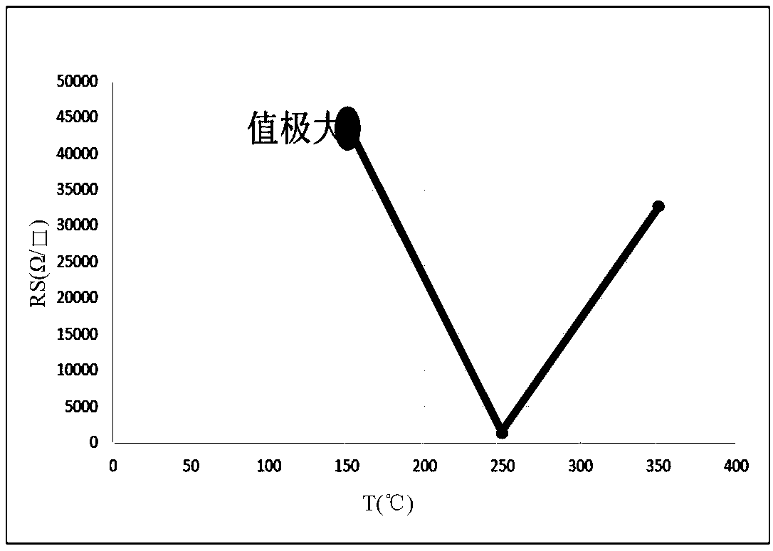
[0040] Due to the high mobility of metal oxides, they are more and more widely used in thin film transistors. However, metal oxides cannot replace metal materials due to their electrical conductivity. As a result, the source and drain electrodes of thin film transistors and the active layer need to be manufactured in different film-forming chambers, which reduces the production efficiency of products and increases production costs.

[0041] In order to solve the above technical problems, the present invention provides a method for manufacturing a thin film transistor, comprising:

[0042] Forming a source electrode, a drain electrode and an active layer;

[0043] It is characterized in that the steps of forming the source electrode, the drain electrode and the active layer include:

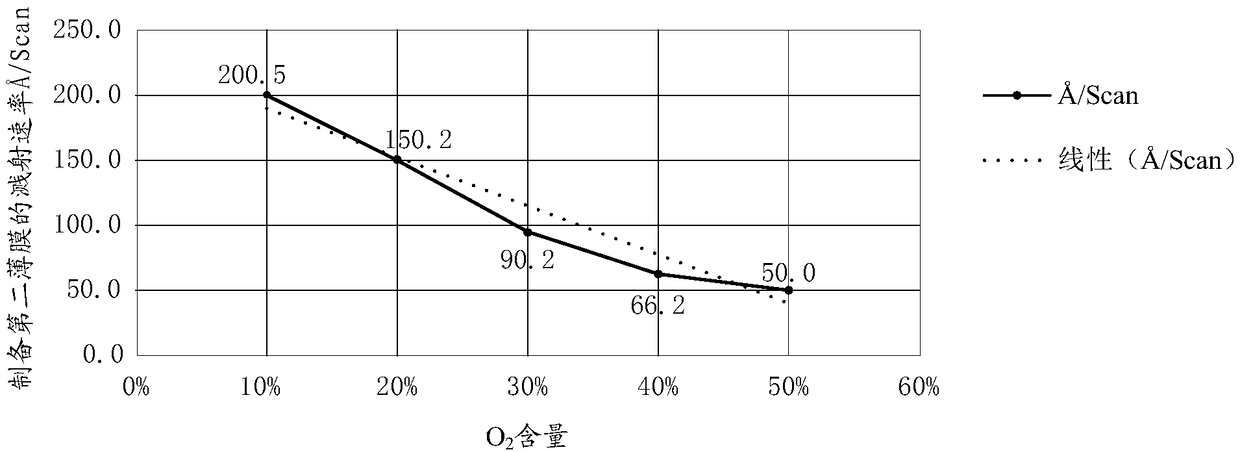
[0044] Under a first preset oxygen content atmosphere, a first film is formed using a first metal oxide material, and under a second preset oxygen content atmosphere, a second film is formed using a


PUM


Abstract

The invention relates to the technical field of display, and discloses a thin film transistor and a manufacturing method thereof and a display substrate. According to the manufacturing method of the thin film transistor, the oxygen content during film forming of a metal oxide material is reduced, so that the square resistivity of the formed film can be lowered, and the requirements of a conductivematerial can be met; and therefore, a source electrode and a drain electrode of the thin film transistor can be manufactured through the metal oxide, so that the source electrode and the drain electrode can be prepared in the same film-forming chamber as an active layer, and a film forming equipment cavity for preparing the source electrode and the drain electrode is omitted, thereby improving the production efficiency of the thin film transistor and lowering the production cost of the display substrate.

Description


Claims


Application Information

Patent Timeline
Owner BOE TECH GRP CO LTD
Why Eureka
Try Eureka