Reflective display device and manufacturing method thereof
A reflective display and reflective liquid technology, which is applied in nonlinear optics, instruments, optics, etc., can solve the problems of poor reflectivity of reflective display devices, etc.
- Summary
- Abstract
- Description
- Claims
- Application Information
AI Technical Summary
Problems solved by technology
Method used
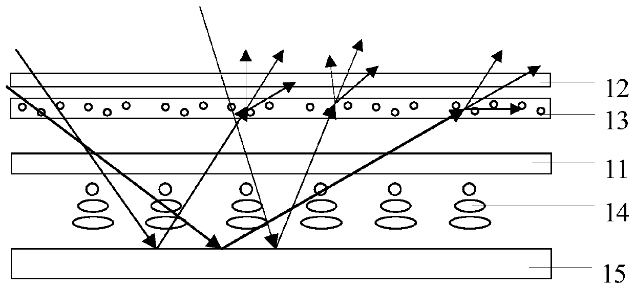
Image

Examples
Embodiment 1
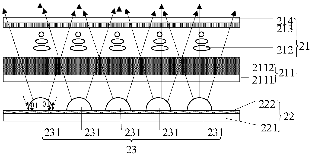
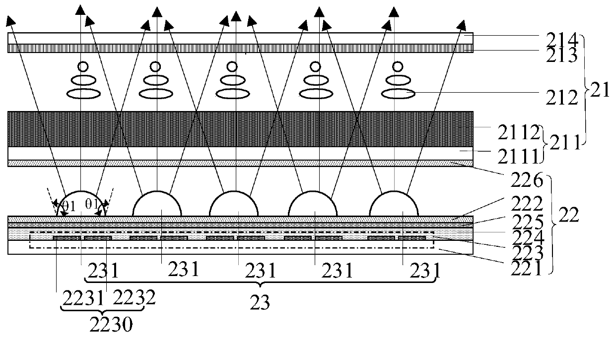
[0042] refer to figure 2 , showing a schematic structural view of a reflective display device according to an embodiment of the present invention, image 3 A schematic structural diagram of another reflective display device according to an embodiment of the present invention is shown.
[0043] An embodiment of the present invention provides a reflective display device, including: a display panel 21, a microfluidic device 22 arranged on the opposite side of the display panel 21 from the light emitting side, and a droplet layer 23 arranged in the microfluidic device 22. The droplet layer 23 includes a plurality of reflective droplets 231 ; the reflective droplets 231 are configured to reflect light incident on the reflective droplets 231 .
[0044] Wherein, the reflective droplet 231 is an organic polymer doped with metal ions, and the metal ions are silver ions.
[0045] The reflective droplet 231 is formed by doping silver ions in the organic polymer, so that the reflective dr
Embodiment 2
[0071] refer to Figure 7 , which shows a flow chart of a method for manufacturing a reflective display device according to an embodiment of the present invention, which may specifically include the following steps:
[0072] Step 701, providing a display panel.
[0073] In the embodiment of the present invention, when fabricating a reflective display device, it is first necessary to fabricate a display panel 21, which is a transmissive display panel. Specifically, first fabricate functional film layers 2112 on the second substrate 2111, Such as thin film transistors, etc., to form a transmissive array substrate 211, and then inject liquid crystal on the transmissive array substrate 211 to form a liquid crystal layer 212, and then align the transmissive array substrate 211 formed with the liquid crystal layer 212 and the color filter substrate 213 After the box alignment is completed, the polarizer 214 is pasted on the color filter substrate 213 to obtain the display panel 21 .
PUM
 Abstract
Description
Claims
Application Information
 - R&D Engineer
- R&D Manager
- IP Professional
- Industry Leading Data Capabilities
- Powerful AI technology
- Patent DNA Extraction
Browse by: Latest US Patents, China's latest patents, Technical Efficacy Thesaurus, Application Domain, Technology Topic.
© 2024 PatSnap. All rights reserved.Legal|Privacy policy|Modern Slavery Act Transparency Statement|Sitemap