Ultraviolet detector and preparation method thereof
An ultraviolet detector and oxide film layer technology, applied in the field of ultraviolet detectors, can solve the problems of complicated circuit connection operation, easily damaged circuit structure, affecting device performance, etc., achieving easy control, ensuring excellent performance, and broad market prospects Effect
- Summary
- Abstract
- Description
- Claims
- Application Information
AI Technical Summary
Benefits of technology
Problems solved by technology
Method used
Image

Examples
preparation example Construction
[0039] The present invention also provides a method of preparing an ultraviolet detector, comprising the steps of:
[0040] a) Set a pixel dot array structure and a readout circuit on the surface of the substrate, the pixel dot array structure being composed of a plurality of pixel units;
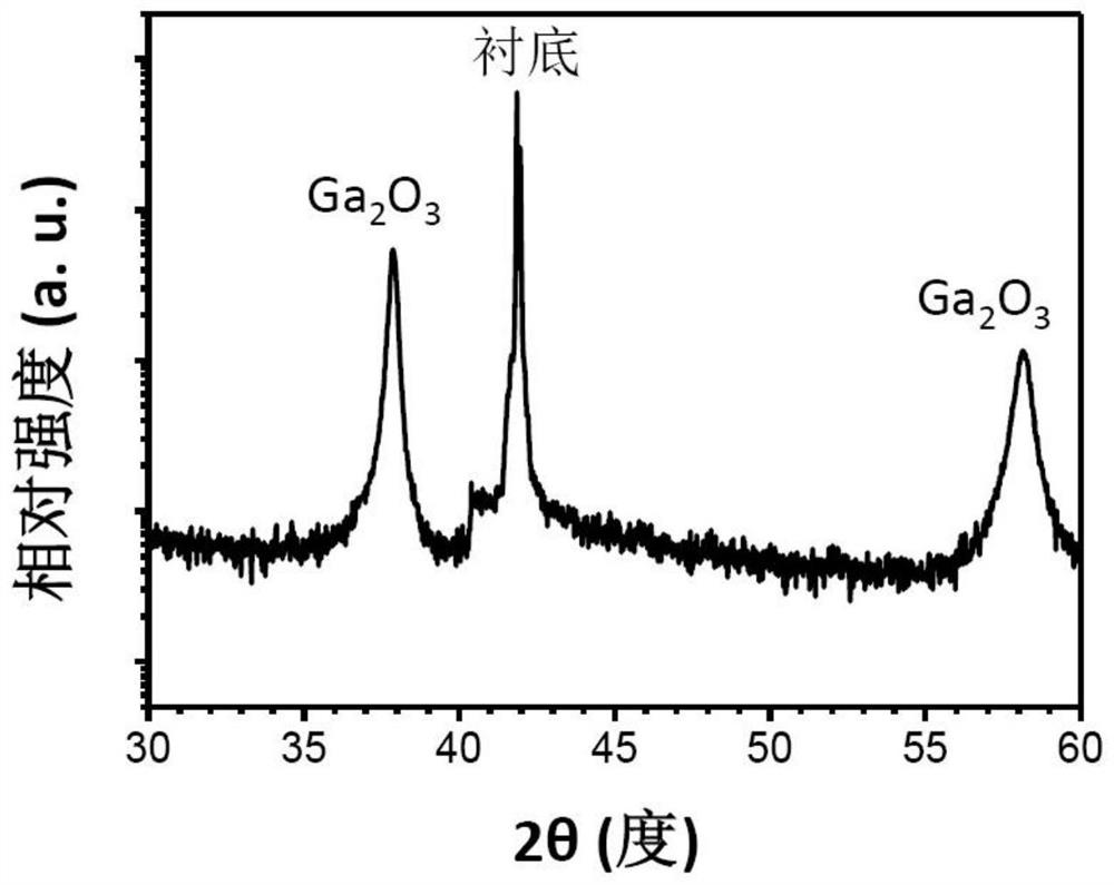
[0041] b) Place the substrate provided with the pixel dot matrix structure and the readout circuit in a wide apparatus for a wide apparatus; use mask to block the reading circuit, and perform a wide-proof with oxide under 20 to 450 ° C. The growth of the membrane layer;
[0042] c) After the growth of the coated oxide film layer is completed, the oxide film grown between adjacent two pixel units is etched off to obtain an ultraviolet detector.
[0043]In the preparation method provided by the present invention, a pixel dot array structure and a readout circuit are first set on the surface of the substrate. Wherein, the substrate includes, but is not limited to, a sapphire substrate; the pixel dot
Embodiment 1
[0051] The ultraviolet detector is prepared, and the specific steps are as follows:
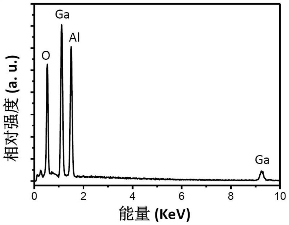
[0052] 1) A 3 × 3 pixel dot structure and a readout circuit are made on the sapphire substrate; wherein each pixel unit in the pixel dot array structure consists of two separate electrode units, the electrode unit consisting of gold. It consists, for the fork finger structure, the finger is 0.5mm, the pointing and finger spacing is 10 μm, and the fork refers to the logarithm of 50 pairs; the readout circuit is connected to each of the pixel units, respectively (the read There are two contacts, each contact corresponding to an electrode unit in the pixel unit), and the material used is a gold portion having a diameter of 25 μm;
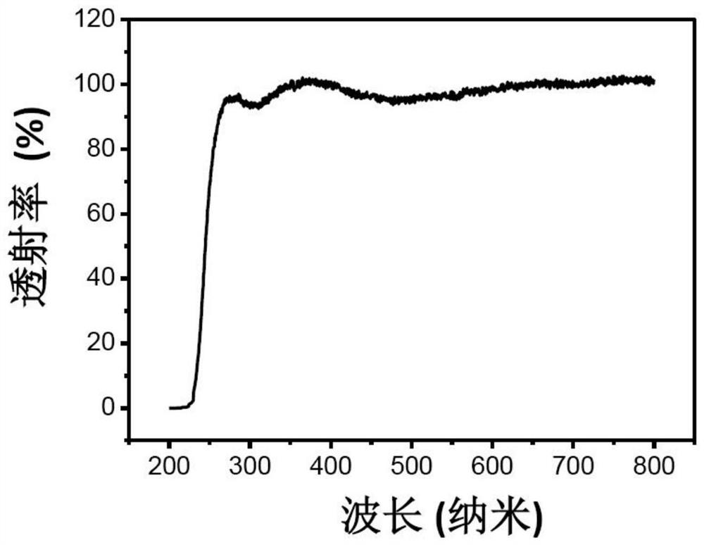
[0053] 2) Place the surface of the surface of the pixel dot matrix structure and the readout circuit in the MOCVD growth apparatus, block the reading circuit with the mask, and only expose the area of the pixel dot matrix, adjust the growth temperature 350 ° C, growth room
Embodiment 2
[0065] Referring to the preparation step of Example 1, the difference is only that GA 2 O 3 The film growth mode is replaced by MOCVD to magnetron sputtering. The specific magnetron sputter condition is: the sputtering radical power is 100 W, the sputtering pressure is 1 × 10 -1 PA, the sputtering time is 2 h; the substrate material grown by the film layer will gradually be sealed to room temperature, and the temperature elimination is preferably naturally cooled.
[0066] Referring to the test method of Example 1, the photoelectric characteristics of the ultraviolet detector prepared by the present embodiment were tested by the readout circuit on the substrate, and the optical current and response time of all 9 pixel units were shown in Table 2:
[0067]Table 2 Photoelectric characteristics of each pixel unit of the ultraviolet detector in Example 2
[0068]
[0069]
[0070] As can be seen from Table 2, the photoelectric characteristics of all 9 pixel units are close to, indica
PUM
| Property | Measurement | Unit |
|---|---|---|
| Diameter | aaaaa | aaaaa |
| Dark current | aaaaa | aaaaa |
Abstract
Description
Claims
Application Information
 - R&D Engineer
- R&D Manager
- IP Professional
- Industry Leading Data Capabilities
- Powerful AI technology
- Patent DNA Extraction
Browse by: Latest US Patents, China's latest patents, Technical Efficacy Thesaurus, Application Domain, Technology Topic.
© 2024 PatSnap. All rights reserved.Legal|Privacy policy|Modern Slavery Act Transparency Statement|Sitemap