Transmitting layer depositing organic luminous display device

A technology of light-emitting display and emission layer, which is applied in lighting devices, electroluminescent light sources, light sources, etc., to achieve the effect of increasing production volume

Inactive Publication Date: 2004-01-28
EASTMAN KODAK CO
View PDF29 Cites 3 Cited by
  • Summary
  • Abstract
  • Description
  • Claims
  • Application Information

AI Technical Summary

Benefits of technology

This patented technology helps create very small emitting layers (EL) at high speeds while also being able to accurately measure their location on various types of displays like LCD screens. It does this by controllably changing the distance between two electrodes used during formation of these tiny structures. Additionally, there are several technical features described such as allowing flexibility in terms of how they work over time based upon factors like ambient temperatures. Overall, this new process results in improved efficiency and consistency across multiple manufacturing processes.

Problems solved by technology

Technological Problem addressed in this patented technical solution described in these documents relates to improving the precision and consistency during construction of displays made up of multiple different types of materials like organic LED' s emitter/electrodes, liquid crystal cells, etc., especially at sizes greater than 100 mm due to limitations associated with current methods used for achieving higher levels of detail control over each component area within the display. Current techniques involve complex processes involving etching, deposition, lithography, printing, and assembly onto small panels, making them expensive and limited in their ability to custom fit into specific shapes needed without being affected negatively.

Method used


Image

  • Transmitting layer depositing organic luminous display device
  • Transmitting layer depositing organic luminous display device
  • Transmitting layer depositing organic luminous display device

Examples


Embodiment Construction

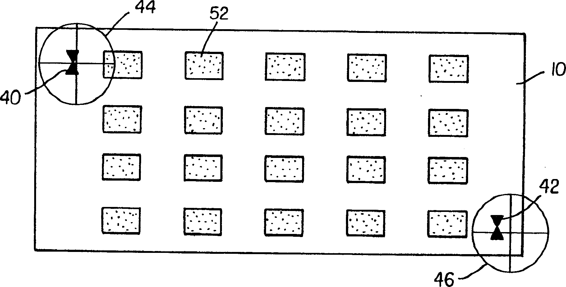
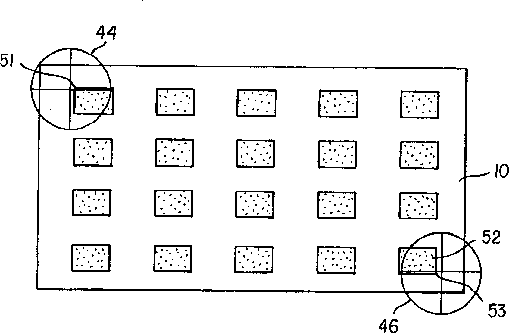
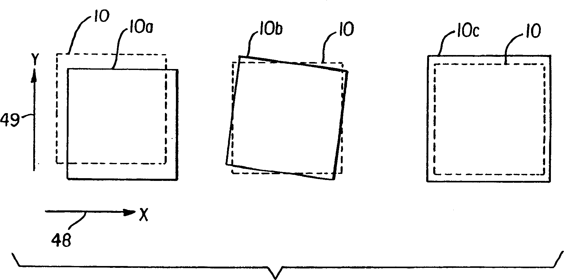
[0034]The term "display" or "display panel" is used to refer to a screen capable of electronically displaying video images or text. The term "pixel" is used in its field-recognized usage to indicate an area of ​​the display panel that can be excited to emit light independently of other areas. The term "OLED device" is used in the meaning of a display device including organic light-emitting diodes as pixels recognized in the field. The color OLED device emits light of at least two colors. The term "multicolor" is used to describe a display panel capable of emitting light of different tones in different areas. In particular, it is used to describe a display panel capable of displaying color images. These areas do not have to be continuous. The term "full color" is used to describe a multi-color display panel capable of emitting in the red, green, and blue regions of the visible spectrum and displaying images in a wide range of tones or combinations of tones. The red, green, and blue co


PUM


Abstract

A method for depositing an OLED emissive layer, includes: providing an OLED substrate having at least one discernible feature; providing a beam of light which is transversely and angularly movable; providing an unpatterned donor element including emissive material and having an energy absorbing layer, arranged so that when the donor element is properly positioned relative to the OLED substrate, the beam of light can be absorbed by the energy-absorbing layer to heat the emissive material and cause its transfer; detecting the location of the discernible feature on the OLED substrate relative to the position of the beam to determine the position and orientation of the OLED substrate relative to the beam; angularly moving the beam and then moving the beam in a raster fashion, in accordance with the detected position and orientation of the OLED substrate, and changing the timing of actuation of the light beam as it is moved to different transverse positions.

Description


Claims


Application Information

Patent Timeline
Owner EASTMAN KODAK CO
Why Eureka
Try Eureka