Image sensor package, optical glass therefor and processing method

An image sensor, optical glass technology, applied in the direction of electric solid device, semiconductor device, glass manufacturing equipment, etc., can solve the problems of delamination, moisture or impurity intrusion, sticking, etc., to reduce the difference of thermal expansion coefficient, ensure the reception The effect of the ability of light signals

Inactive Publication Date: 2007-01-31
SILICONWARE PRECISION IND CO LTD
View PDF6 Cites 8 Cited by
  • Summary
  • Abstract
  • Description
  • Claims
  • Application Information

AI Technical Summary

Benefits of technology

This patented technology allows for efficient creation of small packages containing sensors while maintaining their integrity during use. By performing this process after they have been cut down into smaller parts called individual units or chips, there will be fewer problems when connecting them together properly due to differences in coefficients of linear expansion (CTE) compared to other materials like epoxy resin. Additionally, these techniques allow for better protection against damage from external factors such as water vapor and dusts. Overall, this innovation improves the performance and reliability of electronic devices incorporated within imaging systems.

Problems solved by technology

This patented technical problem addressed in this patent relates how to efficiently capture images without contaminating their surroundings during production process for use in various applications like imaging systems. Existing methods involve gluing optically clear epoxy resin onto the surface of the camera's chip before attaching it into place. However, these techniques have limitations when trying to achieve very small dimensions while maintaining sufficient strength against environmental factors such as temperature changes over prolonged periods.

Method used


Image

  • Image sensor package, optical glass therefor and processing method
  • Image sensor package, optical glass therefor and processing method
  • Image sensor package, optical glass therefor and processing method

Examples


Embodiment

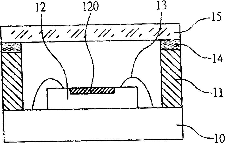
[0017] Figure 3A to Figure 3D is a schematic diagram of the optical glass processing method used in the image sensor package of the present invention.

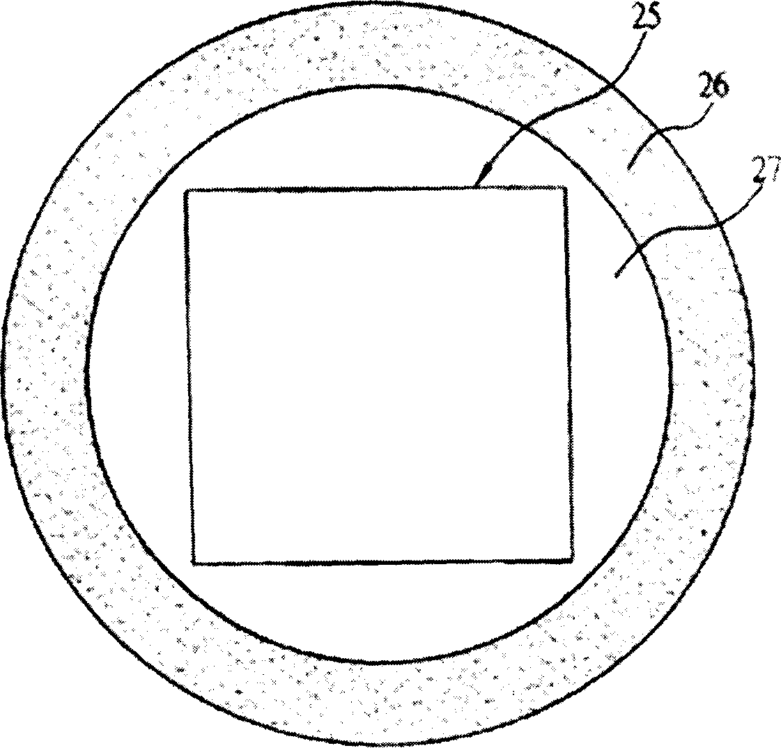
[0018] Such as Figure 3A As shown, a whole piece of optical glass 35 is firstly provided, and a plurality of cutting paths S are pre-divided on the whole piece of optical glass 35 for subsequent cutting operations to form a plurality of optical glass monomers. The entire piece of optical glass 35 can be glued on a tape 37 surrounded by a wafer ring 36 .

[0019] Such as Figure 3B As shown, a grinding tool such as a grinding wheel is used to grind along the cutting path S to form a rough surface 351 on the surface of the cutting path S of the optical glass.

[0020] Such as Figure 3C As shown, it corresponds to Figure 3B A schematic cross-sectional view of the entire piece of optical glass 35 , wherein the rough grinding surface 351 has a depth of about 1 μm to 10 μm, preferably 5 μm, and a width of the rough grinding su


PUM


Abstract

The invention relates to image sensor packaging piece and its optical glass and processing method. The packaging piece includes chip carrier, annular bearing, sensor chip, and optical glass. It includes the following steps: processing grinding before cutting the whole optical glass into many monomers; forming many optical glass monomers with at least one brim rough surface to adhere on the sensor chip bearing to reduce thermal expansion coefficient difference, avoid delaminating caused by thermal stress, prevent moisture and impurity from invading to ensure sensor chip accepting optical signal capacity.

Description


Claims


Application Information

Patent Timeline
Owner SILICONWARE PRECISION IND CO LTD
Why Eureka
Try Eureka