Non-volatile ferroelectric memory device and method of driving the same

a ferroelectric memory and non-volatile technology, applied in semiconductor devices, digital storage, instruments, etc., can solve the problems of narrow refresh margin, increase read time, and inability to reduce the ss value to less than 60 mv/dec, so as to improve the failure rate of unselected memory cells, improve the effect of negative capacitance effect and improve the refresh margin

Active Publication Date: 2019-02-19
SAMSUNG ELECTRONICS CO LTD
View PDF6 Cites 11 Cited by
  • Summary
  • Abstract
  • Description
  • Claims
  • Application Information

AI Technical Summary

Benefits of technology

This patent describes a technology called "passive type” ferroelectric (PRAM) memory devices that can store data without requiring power supply. These devices are designed to operate faster and more efficiently compared to existing technologies like dynamic random access memories (DRAMs). They achieve this by utilizing multiple transistor layers and ferroelectric layers separated by a specific distance. By adjusting the voltages applied to these layers, they can perform different operations depending on whether there is a charge trapped inside the ferroelectric layer or not. Additionally, the technical effects of this technology include improved reliability and performance of the memory device.

Problems solved by technology

The technical problem addressed in this patent is how to prevent interference from unselective memory devices called NAND flash memories while also reducing their energy consumption without sacrificing performance.

Method used


Image

  • Non-volatile ferroelectric memory device and method of driving the same
  • Non-volatile ferroelectric memory device and method of driving the same
  • Non-volatile ferroelectric memory device and method of driving the same

Examples


Embodiment Construction

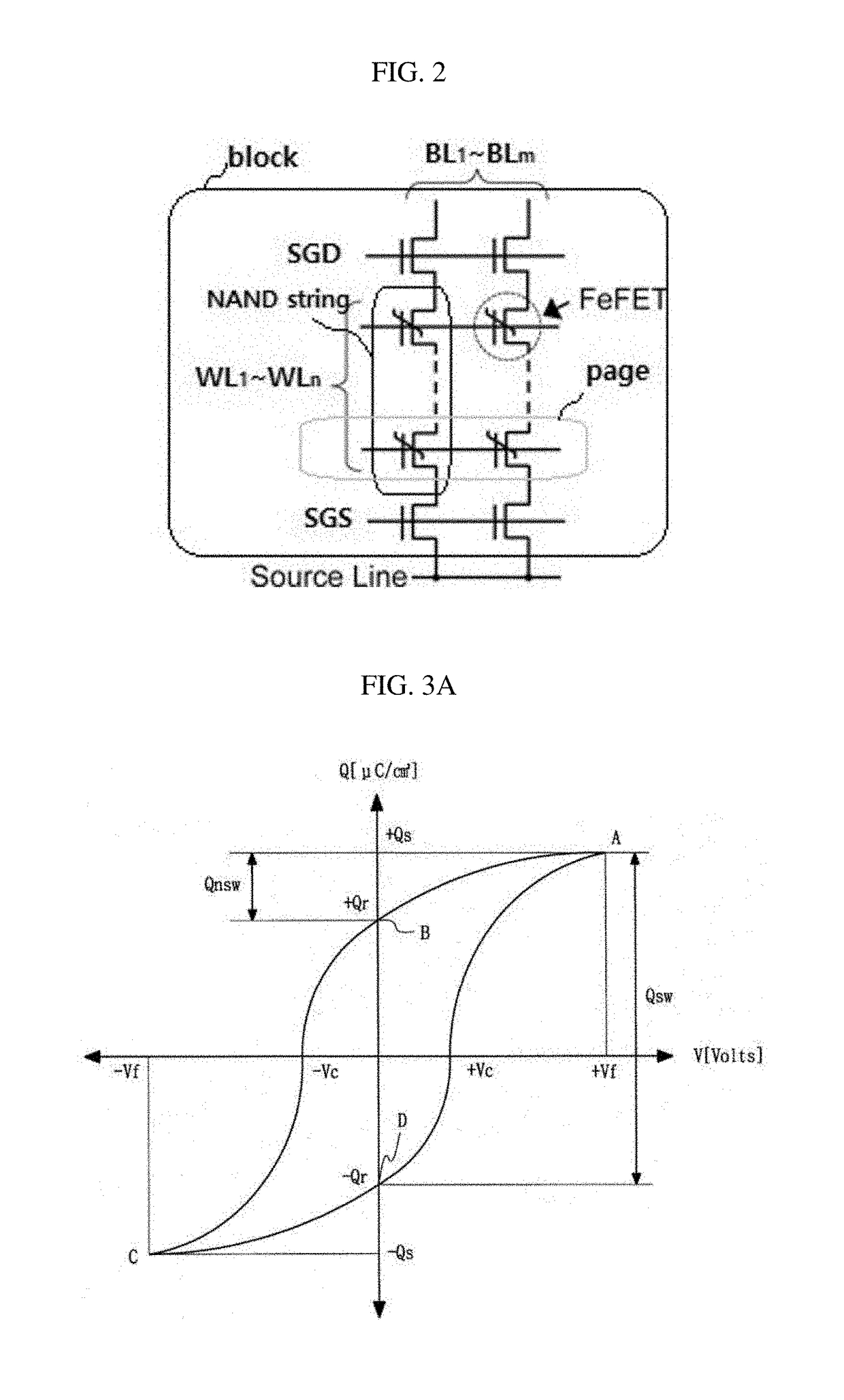
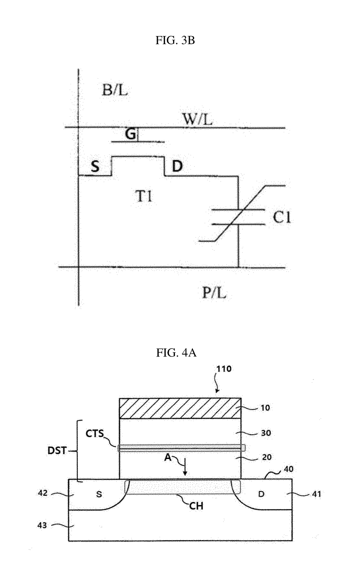
[0030]The present invention now will be described more fully hereinafter with reference to the accompanying drawings, in which embodiments of the invention are shown. This invention may, however, be embodied in many different forms and should not be construed as limited to the embodiments set forth herein. Rather, these embodiments are provided so that this disclosure will be thorough and complete, and will fully convey the scope of the invention to those skilled in the art.

[0031]The terminology used herein is for the purpose of describing particular embodiments only and is not intended to be limiting of the invention. As used herein, the singular forms “a”, “an” and “the” are intended to include the plural forms as well, unless the context clearly indicates otherwise. It will be further understood that the terms “includes”, “comprises” and / or “comprising,” when used in this specification, specify the presence of stated features, integers, steps, operations, elements, and / or compon


PUM


Abstract

The present invention relates to a non-volatile ferroelectric memory device including a semiconductor active layer, a plurality of memory cells connected in series on the semiconductor active layer, and a control circuit for performing a read operation and a program operation on the selected memory cell among the plurality of memory cells, each of the memory cells comprising a para-dielectric layer on the semiconductor active layer; a dielectric stack including a ferroelectric layer stacked on the para-dielectric layer and a charge trap site for generating a negative capacitance effect of the ferroelectric layer by charges disposed and trapped at an interface between the ferroelectric layer and the para-dielectric layer; and a control gate electrode on the ferroelectric layer.

Description


Claims


Application Information

Patent Timeline
Owner SAMSUNG ELECTRONICS CO LTD
Why Eureka
Try Eureka