Method of fabricating a semiconductor device
a semiconductor device and manufacturing method technology, applied in the direction of semiconductor devices, electrical devices, transistors, etc., can solve the problems of destroying all pixels of one column (or one row), complicated drive circuit for driving all the pixels, and forming many tfts
- Summary
- Abstract
- Description
- Claims
- Application Information
AI Technical Summary
Benefits of technology
Problems solved by technology
Method used
Image

Examples
embodiment mode 1
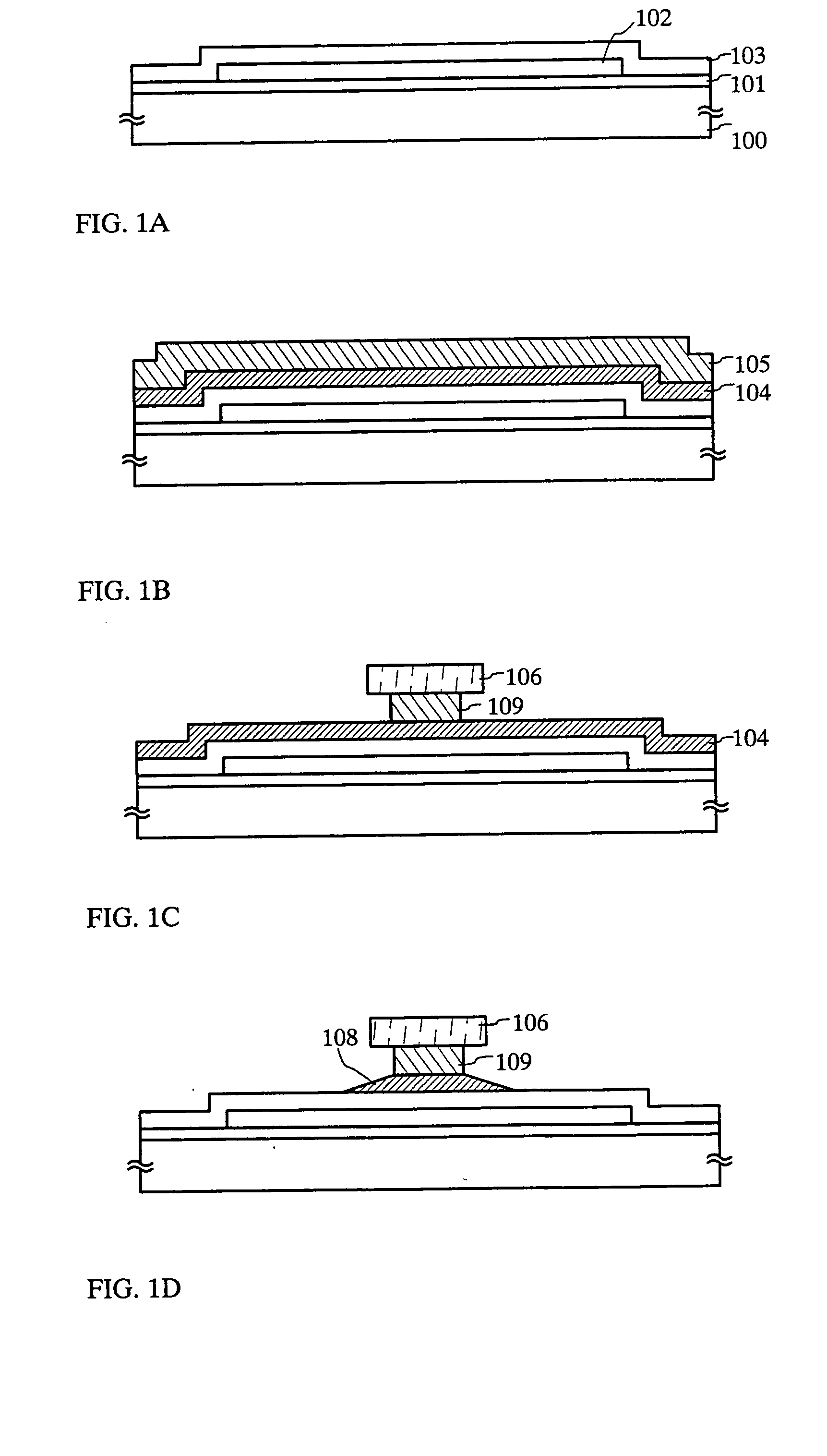
[0072] In this embodiment mode, the present invention is applied to a TFT. Fabricating steps in this embodiment mode will be described with reference to FIGS. 1A to 4D.
[0073] First, an under film 101 is formed on the entire surface of a substrate 100, and an island-like semiconductor layer 102 is formed on the under film 101. An insulating film 103 which becomes a gate insulating film is formed on the entire surface of the substrate 100 to cover the semiconductor layer 102 (FIG. 1A).
[0074] As the substrate 100, a glass substrate, a quartz substrate, a crystalline glass substrate, a stainless substrate, or a resin substrate of polyethylene terephthalate (PFT) etc. may be used.
[0075] The under film 101 is a film for preventing an impurity such as a sodium ion from diffusing from the substrate to the semiconductor layer 102 and for increasing the adhesion of a semiconductor film formed on the substrate 100. As the under film 101, a single-layer or multi-layer film of an inorganic insul
embodiment mode 2
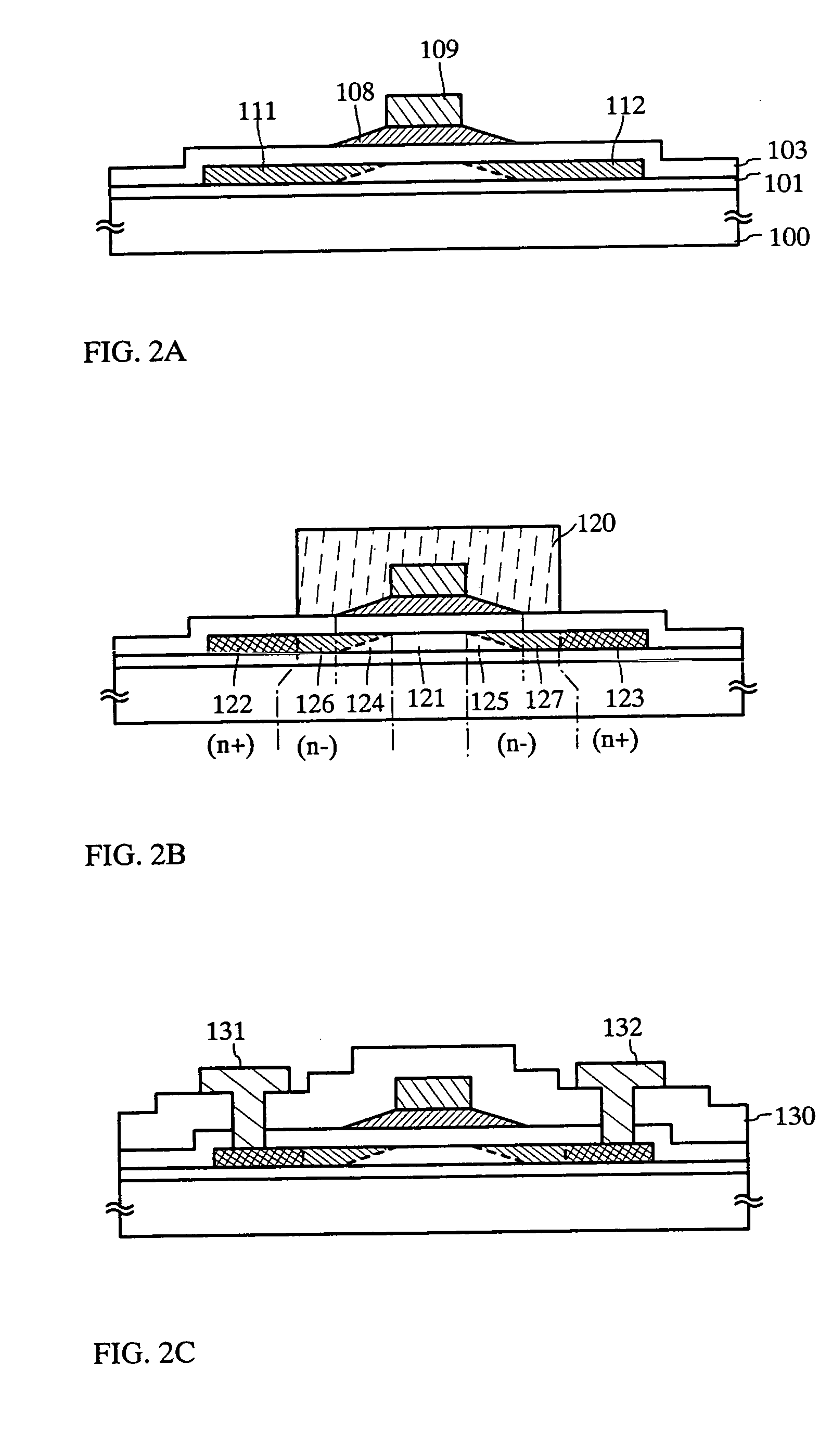
[0115] Fabricating steps of a TFT of this embodiment mode 2 will be described with reference to FIGS. 5A to 5C and FIGS. 6A to 6C. This embodiment mode is a modified example of the embodiment mode 1, in which the structure of a gate electrode (gate wiring line) is modified, and another main structure is the same as the embodiment mode 1.
[0116] Although the gate electrode in the embodiment mode 1 has such a structure that two gate electrodes with different widths are laminated, in this embodiment mode, the upper second electrode is omitted, and the gate electrode is formed of only a first gate electrode having a taper portion.
[0117] First, an under film 141 is formed on the entire surface of a substrate 140, and an island-like semiconductor layer 142 is formed on the under film 141. An insulating film 143 which becomes a gate insulating film is formed on the entire surface of the substrate 140 to cover the semiconductor layer 142 (FIG. 5A).
[0118] A conductive film 144 for making a ga
embodiment mode 3
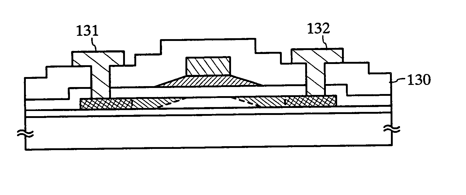
[0132] Fabricating step of a TFT of this embodiment mode will be described with reference to FIG. 7. This embodiment mode is also a modified example of the embodiment mode 1, in which the structure of a gate electrode (gate wiring line) is modified, and another main structure is the same as the embodiment mode 1. Incidentally, in FIG. 7, the same reference numerals as FIGS. 1 and 2 designate the same structural elements.
[0133] Similarly to the embodiment mode 1, although a gate electrode of this embodiment mode 3 has such a structure that a first gate electrode 168 and a second gate electrode 169 are laminated to each other, this embodiment mode is an example in which a side of the first gate electrode 168 is not made taper-shaped. In this embodiment mode, the portion of the first gate electrode 168 extending from the side of the second gate electrode 169 to the outside also has an almost constant film thickness.
[0134] A channel formation region 161, n+-type first impurity regions 16
PUM
 Abstract
Description
Claims
Application Information
 - R&D Engineer
- R&D Manager
- IP Professional
- Industry Leading Data Capabilities
- Powerful AI technology
- Patent DNA Extraction
Browse by: Latest US Patents, China's latest patents, Technical Efficacy Thesaurus, Application Domain, Technology Topic.
© 2024 PatSnap. All rights reserved.Legal|Privacy policy|Modern Slavery Act Transparency Statement|Sitemap