Timing verification method for semiconductor integrated circuit
a technology of integrated circuits and timing verification methods, applied in the direction of instruments, generating/distributing signals, pulse characteristics measurements, etc., can solve the problems of circuit malfunction, increase or decrease in skew, delay in signal propagation, etc., and achieve high reliability
- Summary
- Abstract
- Description
- Claims
- Application Information
AI Technical Summary
Benefits of technology
Problems solved by technology
Method used
Image

Examples
first embodiment
[0062] A timing verification method according to a first embodiment of the present invention will be described with reference to the accompanying drawings.
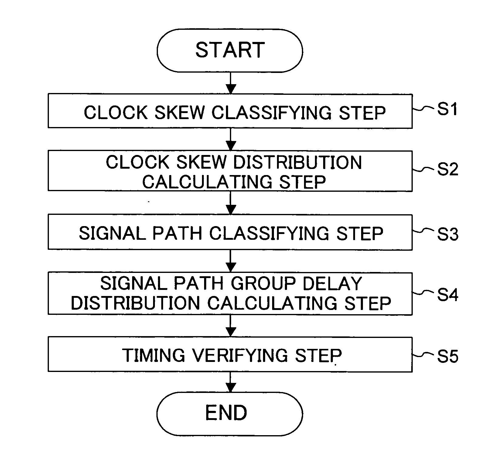
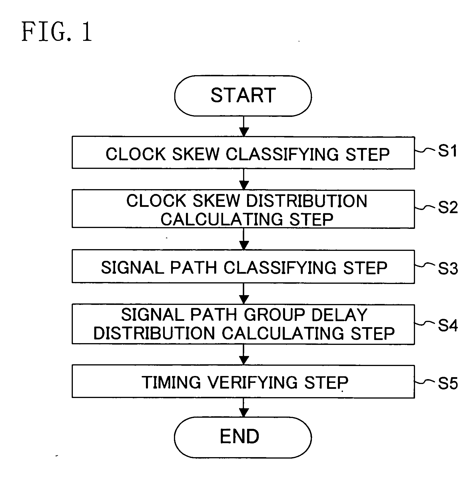
[0063]FIG. 1 illustrates a step flow of the semiconductor integrated circuit timing verification method of the first embodiment of the present invention, including a clock skew classifying step S1, a clock skew distribution calculating step S2, a signal path classifying step S3, a signal path group delay distribution calculating step S4, and a timing verifying step S5.
[0064] (Clock Skew Classifying Step S1)
[0065] Firstly, an idea of handling a skew as a statistical amount using a simple model, and a difference occurring between skew distributions, will be described.
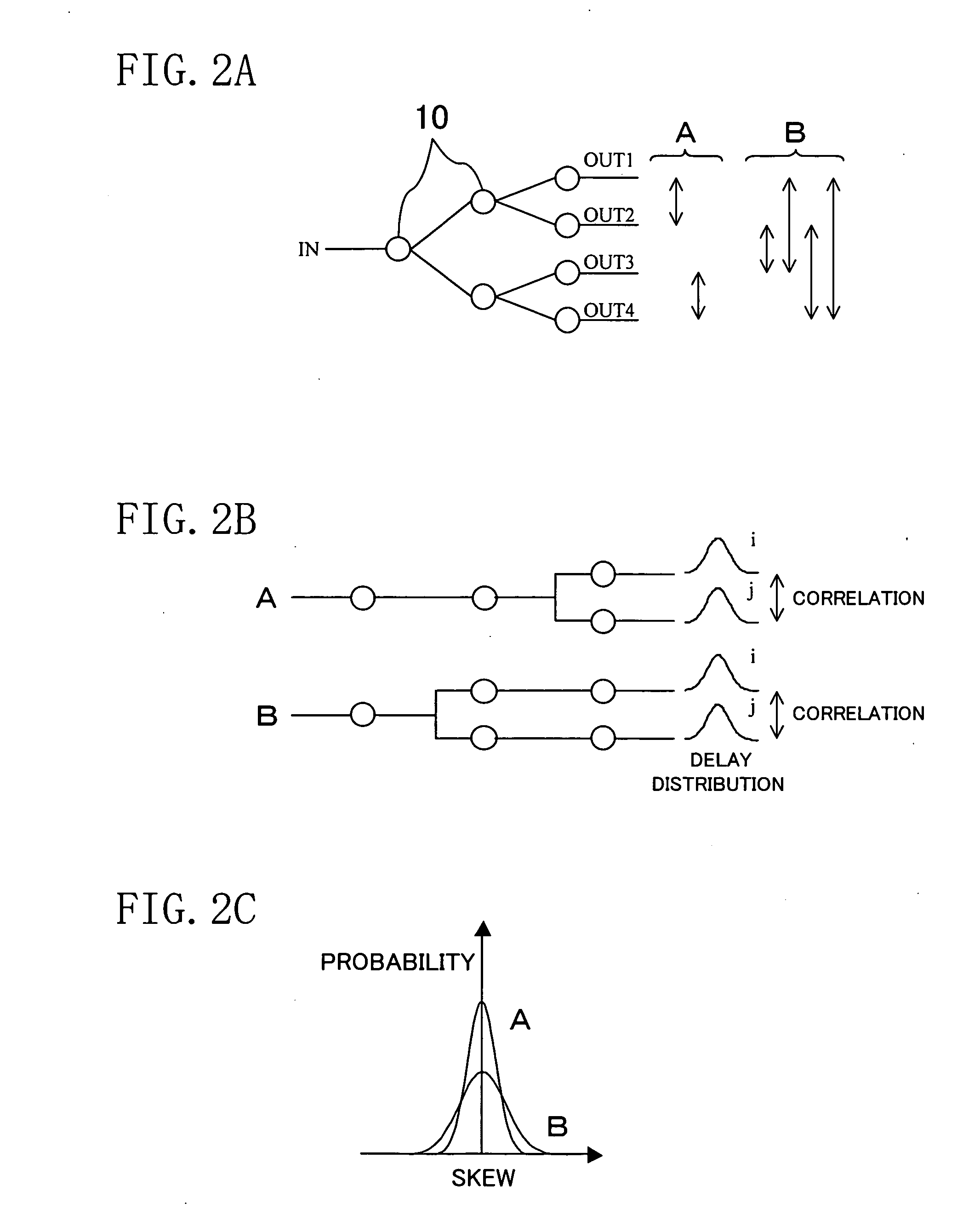
[0066] As illustrated in FIG. 2A, for example, a clock tree circuit is assumed in which a plurality of circuit cells 10, each of which is a buffer having the same configuration, are connected, and all paths from a clock input terminal IN to clock output terminals OUT1
second embodiment
[0112] Hereinafter, a timing verification method according to a second embodiment of the present invention will be described with reference to the drawings.
[0113] In the first embodiment, as illustrated in FIG. 3, the case where there are a plurality of signal paths only between the first clock output terminal pair OUT1 and OUT2 and between the second clock output terminal pair OUT2 and OUT3, corresponding to the inherent skew distributions A and B, respectively, has been described.
[0114] Therefore, as illustrated in FIG. 8A, when a clock tree circuit has a larger number of branches and a larger number of clock signal output terminals than those of FIG. 2A, the second embodiment is enabled.
[0115] It is assumed that a clock signal is supplied from a clock tree circuit to all elements (circuit cells 10) on a chip. In this case, it is also assumed that a correlation between variations of elements close to each other is high, and the correlation decreases with a distance between element
third embodiment
[0121] Hereinafter, a timing verification method according to a third embodiment of the present invention will be described with reference to the drawings.
[0122]FIG. 9 illustrates a step flow of the timing verification method of the third embodiment of the present invention for a semiconductor integrated circuit. As illustrated in FIG. 9, the third embodiment is different from the first embodiment in that the signal path classifying step S3 includes a signal path filtering step S31. Therefore, here, only the signal path filtering step S31 will be described.
(Signal Path Classifying Step S3)
[0123] As illustrated in FIG. 9, in the signal path classifying step S3, a plurality of signal paths in an integrated circuit driven by clock output terminal pairs having skew distributions are classified into the skew distribution types obtained in the clock skew classifying step S1. Note that the signal path classifying step S3 of the third embodiment is different from that of the first embodime
PUM
 Abstract
Description
Claims
Application Information
 - R&D Engineer
- R&D Manager
- IP Professional
- Industry Leading Data Capabilities
- Powerful AI technology
- Patent DNA Extraction
Browse by: Latest US Patents, China's latest patents, Technical Efficacy Thesaurus, Application Domain, Technology Topic.
© 2024 PatSnap. All rights reserved.Legal|Privacy policy|Modern Slavery Act Transparency Statement|Sitemap