Method for manufacturing a semiconductor wafer

a manufacturing method and semiconductor technology, applied in semiconductor/solid-state device manufacturing, basic electric elements, electric devices, etc., can solve the problems of poor flatness of electrodes formed on difficult to remove ground particles by etching, and large number of ground particles that cannot be removed. , to achieve the effect of cleaning the back surface of semiconductor wafers

Inactive Publication Date: 2007-04-26
LAPIS SEMICON CO LTD
View PDF24 Cites 9 Cited by
  • Summary
  • Abstract
  • Description
  • Claims
  • Application Information

AI Technical Summary

Benefits of technology

The technical effect of this patented method is how it helps prevent any unwanted material from sticking on surfaces like those used when processing wafers or removing protective layers made by chemicals called adhesives. This results in better quality finished products with fewer defects than traditional methods without these materials being present at all times.

Problems solved by technology

This technical problem addressed in this patents relates to improving the efficiency at manufacturing electronic devices due to residual particle contamination caused by previous processes used before attaching wafers onto carriages or other components.

Method used


Image

  • Method for manufacturing a semiconductor wafer
  • Method for manufacturing a semiconductor wafer
  • Method for manufacturing a semiconductor wafer

Examples


embodiment

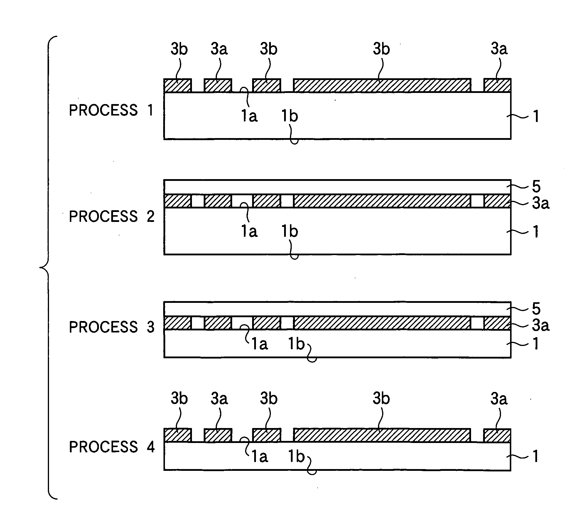
[0023]FIGS. 1 and 2 illustrate a method for manufacturing a semiconductor wafer according to the present invention. Referring to FIGS. 1 and 2, a semiconductor wafer 1 takes the form of a silicon substrate having a front surface la on which a plurality of semiconductor elements 3a (e.g., IGBTs) and surface electrodes 3b. The surface electrodes 3b serve as an anode electrode for the semiconductor elements. A protection tape 5 is a tape having an adhesive-coated side, and is used for use in a back grinding process. The protection tape 5 is attached to the semiconductor wafer 1 by placing the adhesive-coated side on the front surface 1a of the semiconductor wafer 1. The protection tape 5 protects the surface electrodes 3 formed on the front surface 1a of the semiconductor wafer 1 from damage, and prevents ground particles or debris from adhering to the surface electrode 3 during the back grinding process (later described “Process 3”).

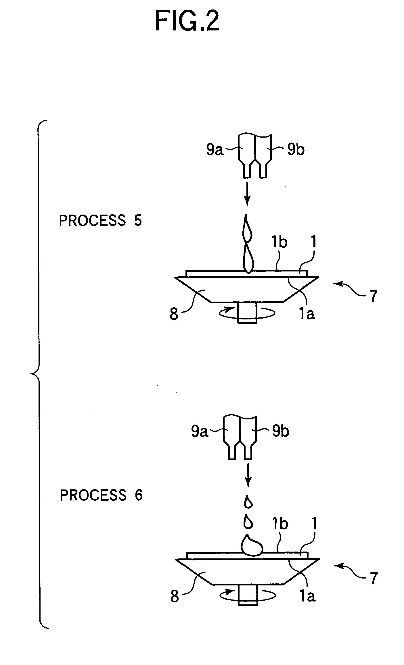
[0024] Referring to FIG. 2, a spin-etching apparatus 7


PUM


Abstract

A method is used for manufacturing a semiconductor wafer. The back surface of a semiconductor wafer is ground. The back surface is cleaned with ozone water. The back surface of the semiconductor wafer is etched with a mixed acid that contains hydrofluoric acid and nitric acid. The cleaning and etching are carried out alternately such that the cleaning and etching are each repeated a plurality of times. The etching is performed after the grinding, beginning when the semiconductor wafer is wet with the ozone water. The cleaning is performed after the etching, beginning when the semiconductor wafer is wet with an etching solution.

Description


Claims


Application Information

Patent Timeline
Owner LAPIS SEMICON CO LTD
Why Eureka
Try Eureka