Organic electroluminescent device
a technology of electroluminescent devices and organic materials, which is applied in the direction of thermoelectric devices, other domestic articles, organic chemistry, etc., can solve the problems of insufficient luminous efficiency of carbazole compounds, excessive holes flowing out to the side of electron transporting layers, and failure to emit light at high efficiency, etc., to achieve good amorphous characteristics, long driving life, and improve stability in various activated states
- Summary
- Abstract
- Description
- Claims
- Application Information
AI Technical Summary
Benefits of technology
Problems solved by technology
Method used
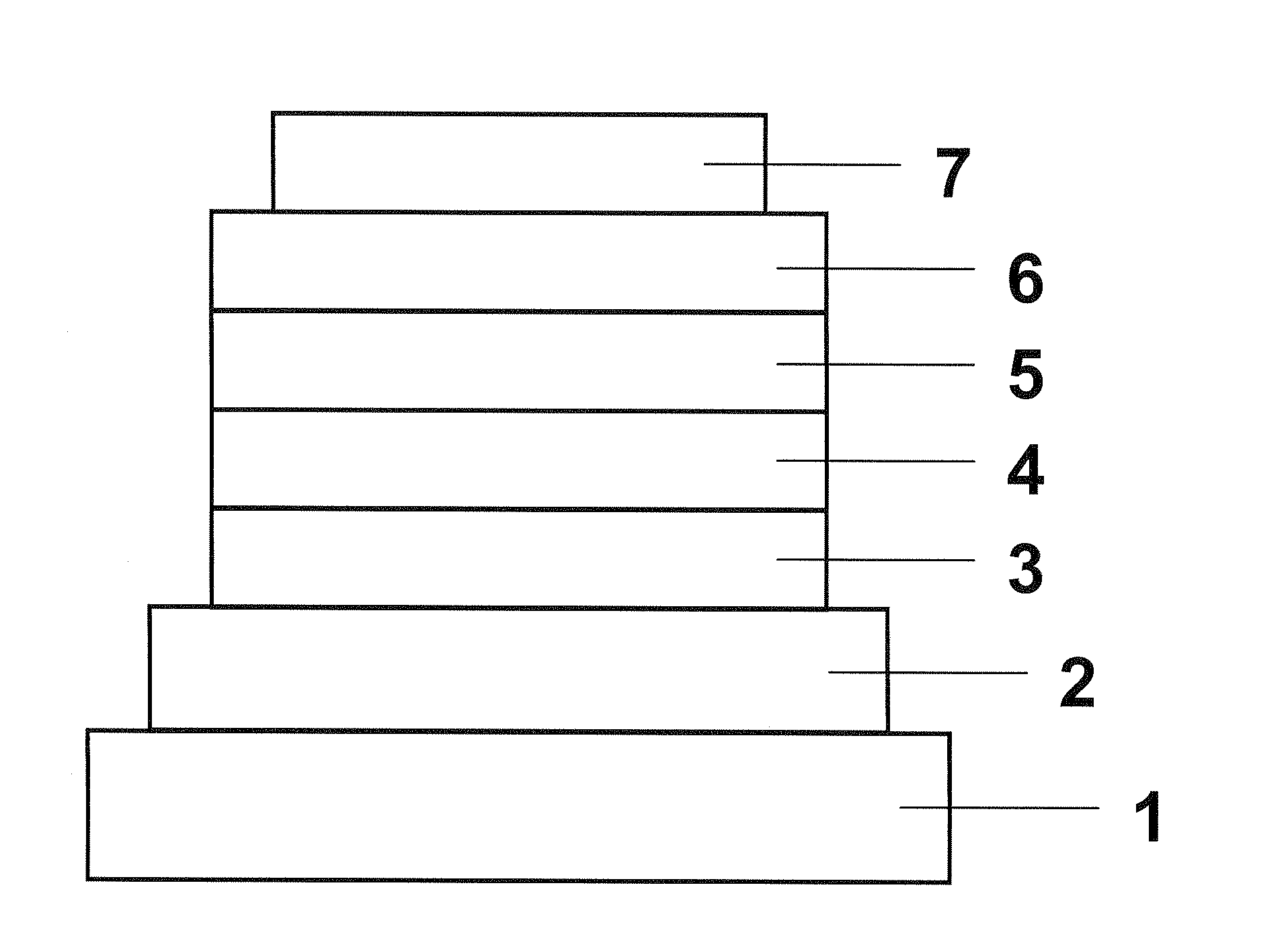
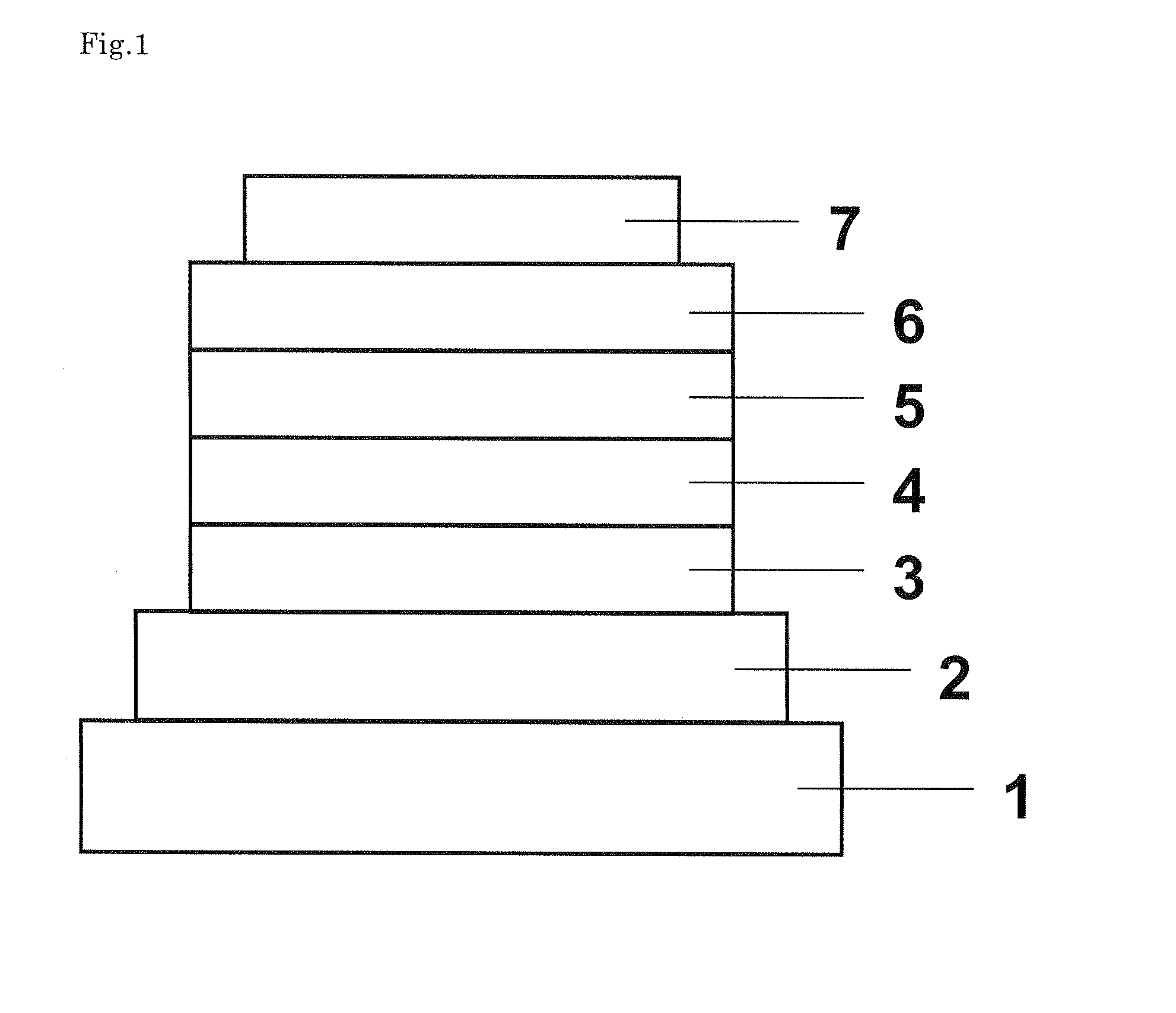
Image

Examples
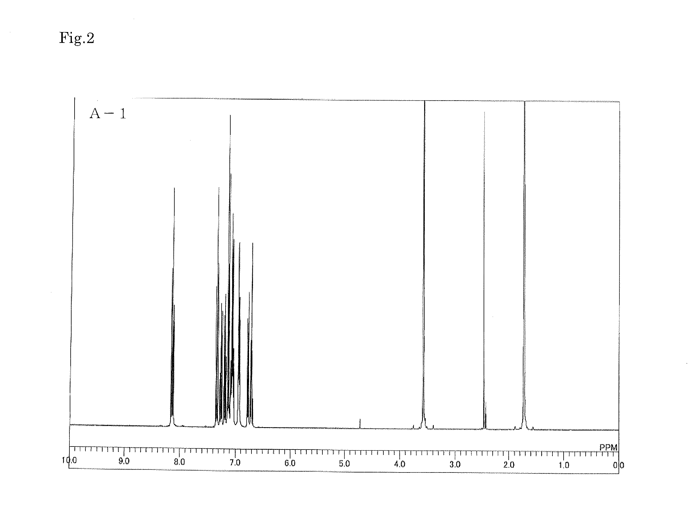
synthetic example 1
Synthesis of Compound A-1
[0082]
[0083]Under a nitrogen atmosphere, 150.0 g (0.671 mol) of 2-bromophenylhydrazine hydrochloride, 190.0 g (1.3 mol) of phthalic anhydride, and 4,500 ml of toluene were mixed and the mixture was heated at 120° C. with stirring overnight. The reaction solution was cooled to room temperature and the precipitated light yellow solid was collected by filtration. The light yellow solid was purified by reslurrying with application of heat to give 181.0 g (0.57 mol, 71% yield) of Intermediate (1) as a light yellow powder.
[0084]Under a nitrogen atmosphere, 126.0 g (0.40 mol) of Intermediate (1), 350.0 g (0.80 mol) of triphenylbismuthine, 108.0 g (0.60 mol) of copper acetate, and 3,000 ml of dehydrated methylene chloride were mixed and the mixture was stirred in an ice bath. To the mixture was slowly added 41.3 ml (0.30 mol) of triethylamine so as to keep the internal temperature from rising above 5° C. and the mixture was heated at 50° C. with stirring overnight. The
example 1
[0089]The constituent layers were deposited in thin film by the vacuum deposition process at a degree of vacuum of 4.0×10⁻⁵ Pa one upon another on a glass substrate on which a 110 nm-thick anode had been formed from ITO. First, copper phthalocyanine (CuPc) was deposited on the ITO anode to a thickness of 20 nm. Then, 4,4′-bis[N-(1-naphthyl)-N-phenylamino]biphenyl (NPB) was deposited to a thickness of 20 nm to form a hole-transporting layer. Next, Compound A-1 as a host material and tris(2-phenylpyridine)iridium(III) (Ir(ppy)3) as a dopant were co-deposited on the hole-transporting layer from different deposition sources to a thickness of 30 nm to form a light-emitting layer. At this time, the concentration of Ir(ppy)3 was 10 wt %. Next, BAlq was deposited to a thickness of 10 nm to form a hole-blocking layer. Then, tris(8-hydroxyquinolinato)aluminum (III) (Alq3) was deposited to a thickness of 40 nm to form an electron-transporting layer. Further, lithium fluoride (LiF) was deposited o
example 2
[0091]An organic EL device was fabricated as in Example 1 except that Compound A-8 was used as the host material in the light-emitting layer.
PUM
 Abstract
Description
Claims
Application Information
 - R&D Engineer
- R&D Manager
- IP Professional
- Industry Leading Data Capabilities
- Powerful AI technology
- Patent DNA Extraction
Browse by: Latest US Patents, China's latest patents, Technical Efficacy Thesaurus, Application Domain, Technology Topic.
© 2024 PatSnap. All rights reserved.Legal|Privacy policy|Modern Slavery Act Transparency Statement|Sitemap