Printed circuit board including electronic component embedded therein and method for manufacturing the same

a technology of printed circuit boards and electronic components, which is applied in the direction of printed circuit non-printed electric components association, sustainable manufacturing/processing, and final product manufacturing, etc., can solve the problems of short circuit, difficult to maximize the flowability of resin leaked from the buildup material in the cavity of the core, and the mounting area of electronic components may not be sufficiently secured, so as to improve the reliability and yield of a product.

Active Publication Date: 2014-10-30
SAMSUNG ELECTRO MECHANICS CO LTD
View PDF3 Cites 14 Cited by
  • Summary
  • Abstract
  • Description
  • Claims
  • Application Information

AI Technical Summary

Benefits of technology

The technical effect that this technology provides is how it can make sure things are done correctly by embedding electronics into certain materials used during production without damaging them or causing damage when they get stuck together due to vibrations caused from machining processes.

Problems solved by technology

The technical problem addressed in this patented text relates how to efficiently embed electronics into limited areas without causing damage during production processes due to their high coefficients of thermal shrinkage compared to other materials used in conventional methods.

Method used


Image

  • Printed circuit board including electronic component embedded therein and method for manufacturing the same
  • Printed circuit board including electronic component embedded therein and method for manufacturing the same
  • Printed circuit board including electronic component embedded therein and method for manufacturing the same

Examples


Embodiment Construction

[0024]The acting effects and technical configuration with respect to the objects of a printed circuit board including an electronic component embedded therein and a method for manufacturing the same according to the present invention will be clearly understood by the following description in which exemplary embodiments of the present invention are described with reference to the accompanying drawings.

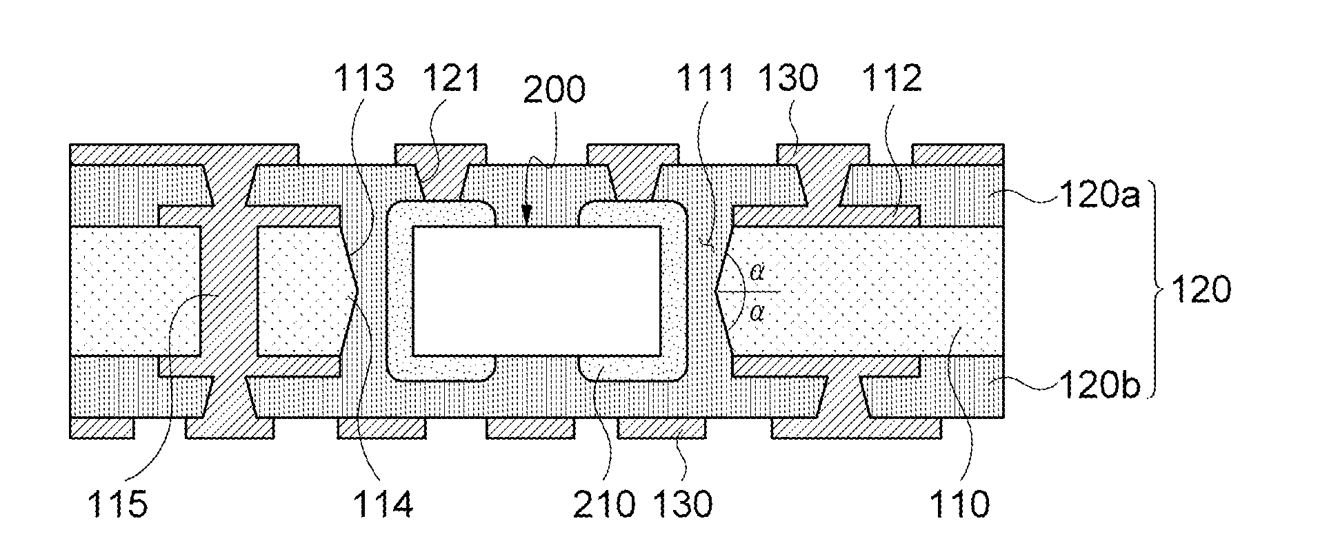
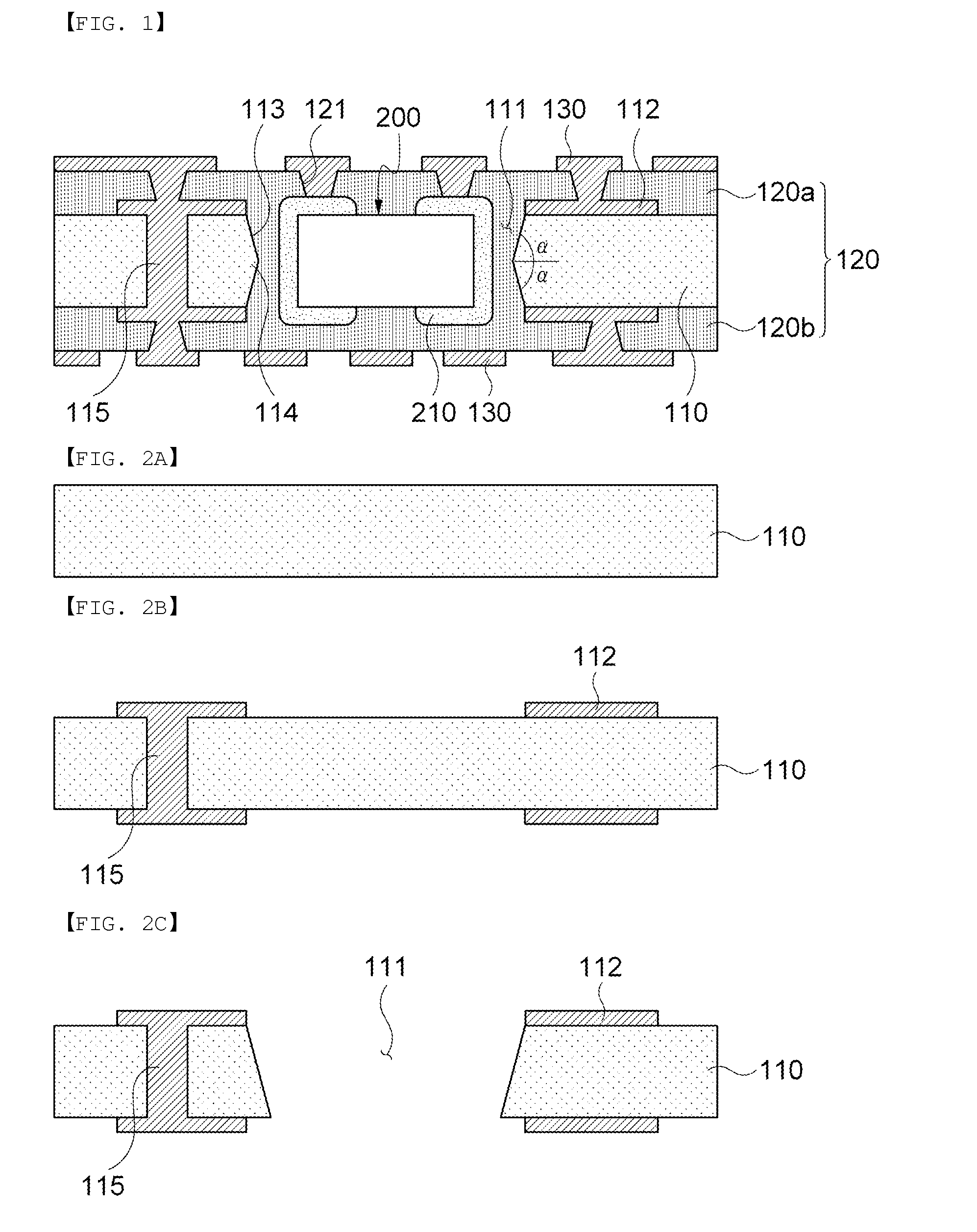
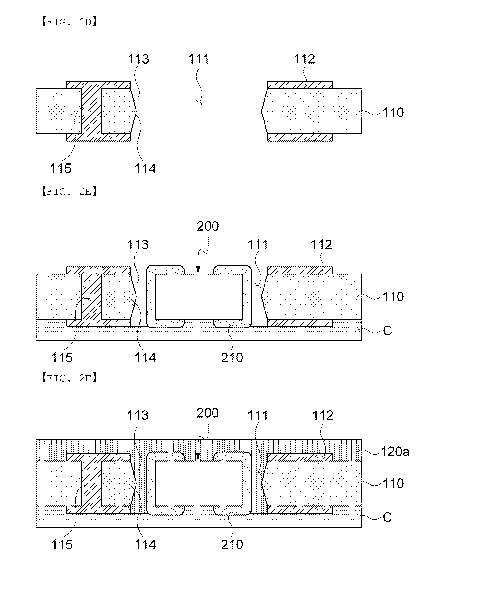
[0025]First, FIG. 1 is a cross-sectional view of a printed circuit board including an electronic component embedded therein according to an exemplary embodiment of the present invention.

[0026]As illustrated in FIG. 1, a printed circuit board 100 including an electronic component embedded therein according to an exemplary embodiment of the present invention may include a core 110 in which a cavity 111 is formed, an electronic component 200 embedded in the cavity 111, an insulating layer 120 stacked on upper and lower portions of the core 110 including the electronic component 200, and exter


PUM

PropertyMeasurementUnit
Angleaaaaaaaaaa
Angleaaaaaaaaaa
Surface roughnessaaaaaaaaaa

Abstract

Disclosed herein are a printed circuit board including an electronic component embedded therein and a method for manufacturing the same. The printed circuit board including an electronic component embedded therein includes: a core formed with a cavity which is formed of a through hole and has a side wall formed with an inclined surface having a top and bottom symmetrically formed based on a central portion thereof; an electronic component embedded in the cavity; insulating layers stacked on upper and lower portions of the core including the electronic component; and external circuit layers formed on the insulating layers.

Description


Claims


Application Information

Patent Timeline
Owner SAMSUNG ELECTRO MECHANICS CO LTD
Why Eureka
Try Eureka