System and method for improving oxide-nitride-oxide (ONO) coupling in a semiconductor device

a technology of oxide-nitride-oxide and semiconductor devices, which is applied in the direction of semiconductor devices, electrical equipment, transistors, etc., can solve the problems that conventional sti fabrication techniques cannot provide suitably efficient and reliable isolation

Active Publication Date: 2010-03-16
GLOBALFOUNDRIES US INC +1
View PDF10 Cites 3 Cited by
  • Summary
  • Abstract
  • Description
  • Claims
  • Application Information

AI Technical Summary

Benefits of technology

This patented technology describes two ways for creating a type of semiconductor device called Non Volatility Random Access Memory (NVRAM). These techniques involve adding isolated areas on top layers or other parts of the chip that separate different components within it from one another. By doing this they can improve their performance without requiring expensive equipment like high voltage power supplies used during manufacturing processes.

Problems solved by technology
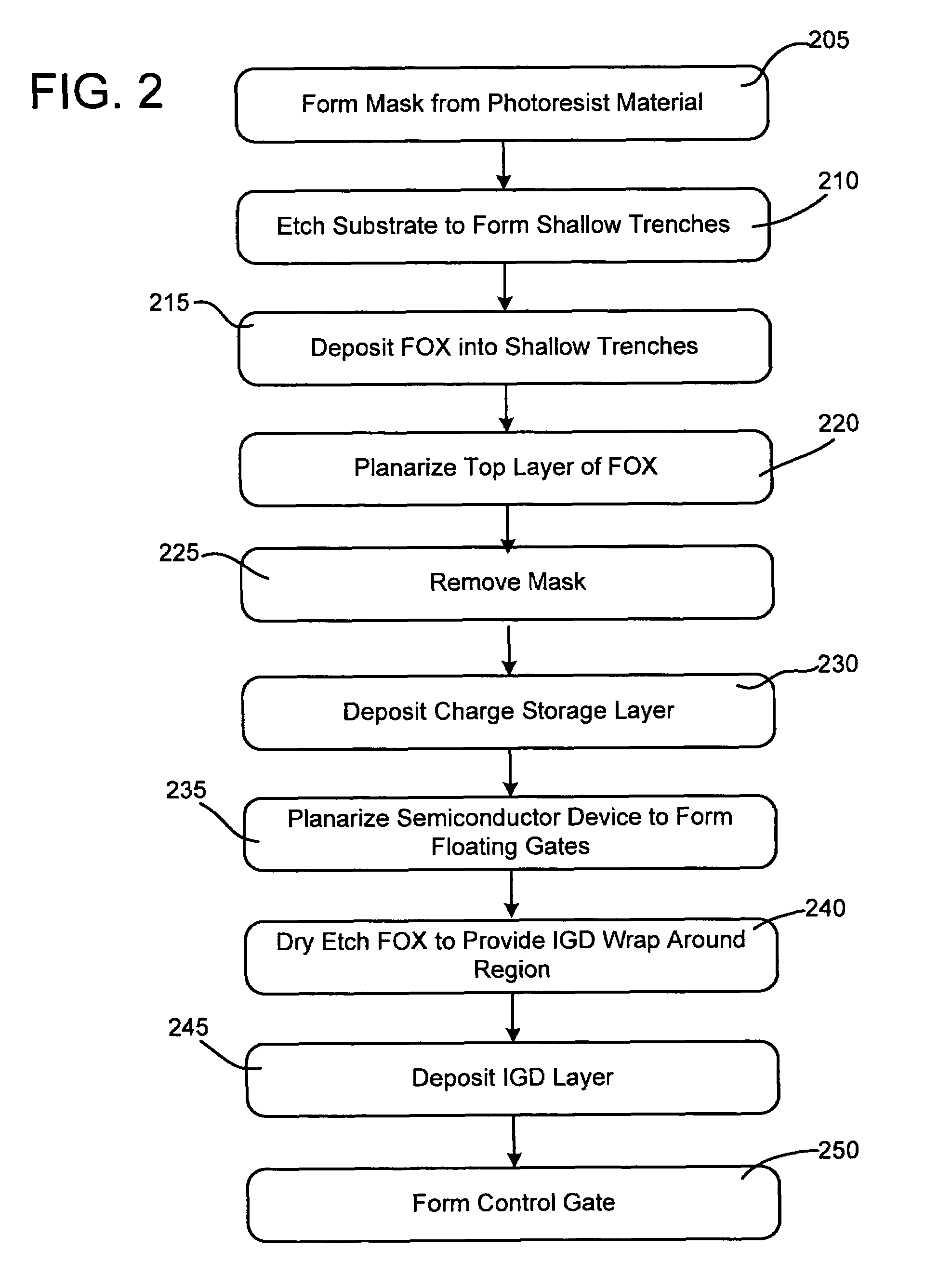
Technological Problem: Controlled Random Access Memories (RAMs), particularly Flash memristive random access memory (FRAM) devices require effective isolations due to their smaller sizes and reduced circuitry area requirements compared to traditional logic designs used today. Current methods like LOCOS isolators cannot achieve sufficient efficiency and reliability while also providing suitable isolation capabilities.

Method used


Image

  • System and method for improving oxide-nitride-oxide (ONO) coupling in a semiconductor device
  • System and method for improving oxide-nitride-oxide (ONO) coupling in a semiconductor device
  • System and method for improving oxide-nitride-oxide (ONO) coupling in a semiconductor device

Examples


Embodiment Construction

[0015]The following detailed description of implementations consistent with the principles of the invention refers to the accompanying drawings. The same reference numbers in different drawings may identify the same or similar elements. Also, the following detailed description does not limit the invention. Instead, the scope of the invention is defined by the appended claims and their equivalents.

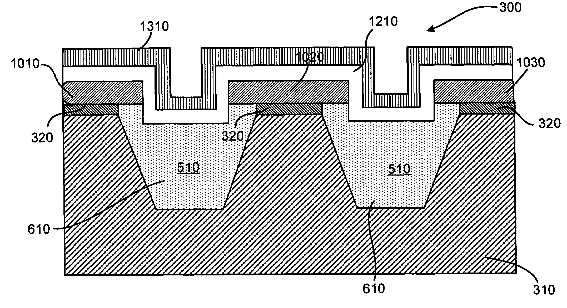
[0016]Implementations consistent with the present invention provide non-volatile memory devices with improved ONO to floating gate coupling, such as flash electrically erasable programmable read only memory (EEPROM) devices. FIG. 1 illustrates an exemplary configuration of a flash EEPROM 100 formed in accordance with an embodiment of the present invention. Flash memory 100 may include a plurality of memory cells 102, arranged in a rectangular matrix or array of rows and columns, a plurality of bit lines (BL) associated with each column, a plurality of word lines (WL) associated with each row,


PUM


Abstract

A memory device includes a substrate and a first dielectric layer formed over the substrate. At least two charge storage elements are formed over the first dielectric layer. The substrate and the first dielectric layer include a shallow trench filled with an oxide material. The oxide material formed in a center portion of the shallow trench is removed to provide a region with a substantially rectangular cross-section.

Description


Claims


Application Information

Patent Timeline
Owner GLOBALFOUNDRIES US INC
Why Eureka
Try Eureka