Mini-LED structure with spliced subarea cells and production process of mini-LED structure

A mini-led, production process technology, applied in the field of LED backlight, can solve the problem of inconvenient removal and replacement of mini-LED chips, and achieve the effect of reducing the probability of de-soldering, less quantity and high production level

Active Publication Date: 2022-03-08
深圳市兆纪光电有限公司
View PDF4 Cites 2 Cited by
  • Summary
  • Abstract
  • Description
  • Claims
  • Application Information

AI Technical Summary

Problems solved by technology

[0005] In order to improve the situation that mini-LED chips are inconvenient to be unsoldered and repla

Method used


Image

  • Mini-LED structure with spliced subarea cells and production process of mini-LED structure
  • Mini-LED structure with spliced subarea cells and production process of mini-LED structure
  • Mini-LED structure with spliced subarea cells and production process of mini-LED structure

Examples


Embodiment Construction

[0049] The following is attached Figure 1-9 The application is described in further detail.

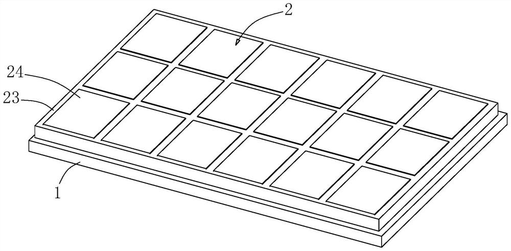
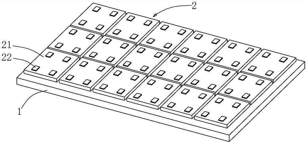
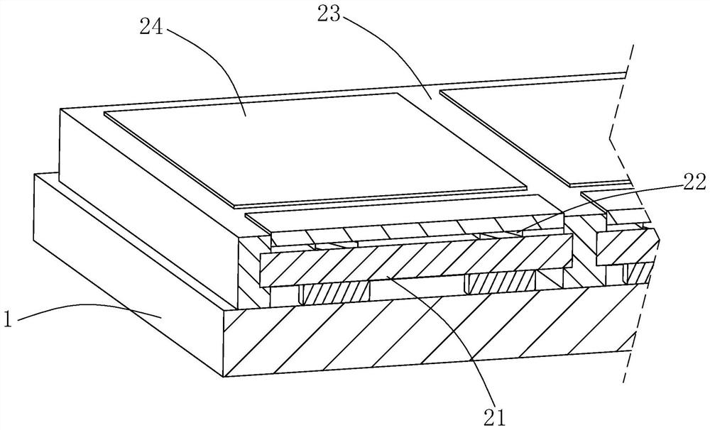
[0050] The embodiment of the present application discloses a mini-LED structure with splicing of partitioned cells. refer to figure 1 with 2 , including a PCB base carrier 1, a plurality of partition cells 2 are arranged on one surface of the PCB base carrier 1, and the partition cells 2 include a PCB partition carrier 21 electrically connected to the surface of the PCB base carrier 1 and a plurality of The mini-LED chips 22, a plurality of mini-LED chips 22 are fixedly connected to a surface of the PCB partition carrier 21 away from the PCB base carrier 1 and the mini-LED chips 22 are electrically connected to the PCB partition carrier 21. If it is found that the mini-LED chip 22 in a certain partition cell 2 cannot work normally, the worker can desolder the PCB partition carrier board 21 of the partition cell 2 and replace it with a new partition cell 2 . The number of mini-LED ch


PUM


Abstract

The invention relates to a mini-LED structure with spliced partition cells and a production process, and belongs to the field of LED backlight, the mini-LED structure comprises a PCB base layer carrier plate, and a plurality of partition cells are arranged on one surface of the PCB base layer carrier plate; the partition unit grid comprises a PCB partition carrier plate and a plurality of mini-LED chips, the PCB partition carrier plate is electrically connected to the surface of the PCB base carrier plate, the mini-LED chips are fixedly connected to the surface, away from the PCB base carrier plate, of the PCB partition carrier plate, and the mini-LED chips are electrically connected with the PCB partition carrier plate. According to the invention, the condition that the mini-LED chip is inconvenient to deweld and replace is improved.

Description


Claims


Application Information

Patent Timeline
Owner 深圳市兆纪光电有限公司
Why Eureka
Try Eureka