Multilayer wiring board and power supply structure to be embedded in multilayer wiring board

a multi-layer wiring board and power supply technology, applied in pulse generators, printed circuit non-printed electric components association, pulse technique, etc., can solve problems such as reducing electrical resistance, and achieve the effects of low resistance, high current, and large power

Inactive Publication Date: 2008-06-26
NGK SPARK PLUG CO LTD
View PDF3 Cites 58 Cited by
  • Summary
  • Abstract
  • Description
  • Claims
  • Application Information

AI Technical Summary

Benefits of technology

The present invention relates to a power supply system for electronic devices. It includes a conductive metal plate called a copper rod that connects to both the conductive metal tape and the conductive metal tube. By inserting these components together, they create multiple current paths within the power supply structure, allowing for efficient supplying of high currents without increasing its size. Additionally, it provides a stable electrical connection from the main surface side to the backside conductor layer for power supply purposes. Overall, this design allows for effective operation of electronic devices and reduces interference caused by power supply noise.

Problems solved by technology

The technical problem addressed in this patent is how to efficiently supply high currents to electronic devices while maintaining their functionality without increasing the size of the device itself. This requires a larger number of through holes per unit area in the substrate, but traditional methods have limitations due to the use of copper plating to form through holes.

Method used


Image

  • Multilayer wiring board and power supply structure to be embedded in multilayer wiring board
  • Multilayer wiring board and power supply structure to be embedded in multilayer wiring board
  • Multilayer wiring board and power supply structure to be embedded in multilayer wiring board

Examples


Embodiment Construction

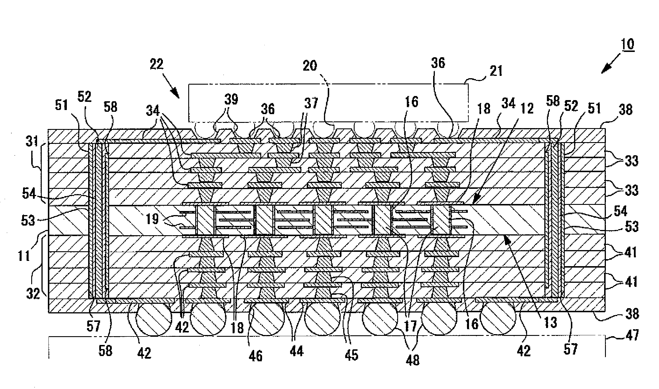
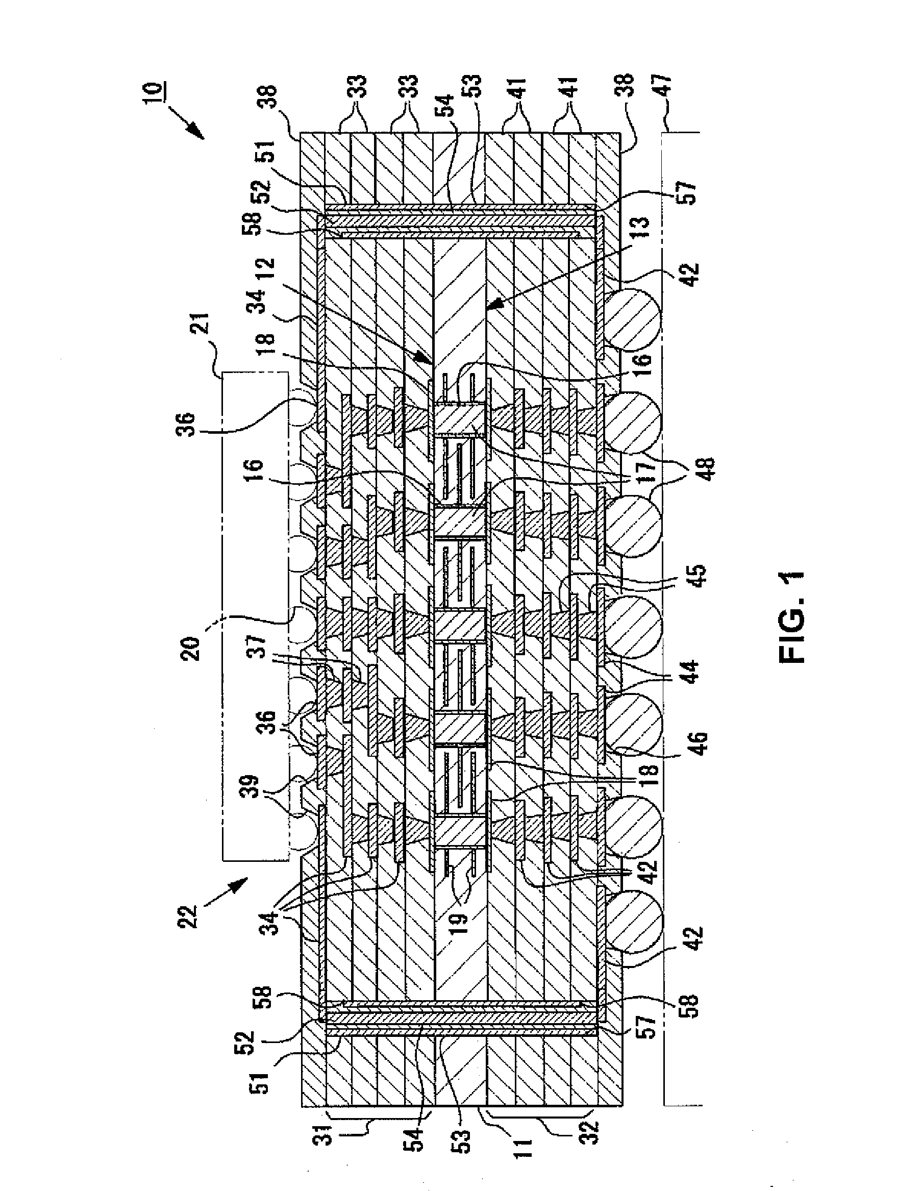
[0063]An embodiment for carrying out a multilayer wiring board of the present invention will be described in detail with reference to the drawings. FIG. 1 is a schematic sectional view showing a multilayer wiring board 10 according to an embodiment of the invention.

[0064]As shown in FIG. 1, the multilayer wiring board 10 is a wiring board for mounting an IC chip thereon and is comprised of: a generally rectangular core board 11 made of glass epoxy; a build up layer 31 (first laminated wiring portion) formed on an upper surface 12 (main surface) of the core board 11; and a build up layer 32 (second laminated wiring portion) formed on a lower surface 13 (rear surface) of the core board 11. Through hole conductors 16 are formed at a plurality of locations in the core board 11. These through hole conductors 16 are formed by applying a copper plating to an inner circumference of a through hole to thereby electrically connect the upper surface 12 and the lower surface 13 of the core board 11


PUM

PropertyMeasurementUnit
Diameteraaaaaaaaaa
Electrical resistanceaaaaaaaaaa
Electrical conductoraaaaaaaaaa

Abstract

A multilayer wiring board capable of feeding sufficient electric power to a circuit element, such as an IC chip. In one embodiment of the present invention, a multilayer wiring board is comprised of: a core board; a build up layer disposed on an upper surface of the core board; a build up layer disposed on a lower surface of the core board; and a power supply structure embedded in a through hole penetrating the core board and the build up layers. The power supply structure is comprised of: a conductive metal rod made of copper as a main material; a conductive metal tube made of copper as a main material and provided coaxially with the conductive metal rod; and an insulating material filling a gap between the conductive metal rod and the conductive metal tube.

Description


Claims


Application Information

Patent Timeline
Owner NGK SPARK PLUG CO LTD
Why Eureka
Try Eureka