Sputter etch processing for heavy metal patterning in integrated circuits

a technology of integrated circuits and etching profiles, which is applied in the direction of semiconductor devices, semiconductor/solid-state device details, electrical apparatus, etc., can solve the problems of reentrant reactive ion etching profiles, poor liner/seed coverage on the walls of trenches, and damascene processing that is not always compatible with the trend toward smaller feature sizes

Active Publication Date: 2014-09-18
APPLIED MATERIALS INC +1
View PDF5 Cites 7 Cited by
  • Summary
  • Abstract
  • Description
  • Claims
  • Application Information

AI Technical Summary

Benefits of technology

The present invention relates to methods for making multiple conductive lines on an integrated circuit with improved efficiency and reliability. These techniques involve creating layers of copper containing conductive metals on top of a substrate, followed by forming patterns using different types of plasmas. This allows for better control over the formation of these conductive paths, resulting in higher performance and reliability of the overall device.

Problems solved by technology

This patent describes a problem when trying to create fine wires in integrated circuitry by depositing copper onto an insulation material called silica. Current methods result in incomplete or imperfect copper fillings due to issues like uneven distribution of copper atoms along the sides of the trenches, difficulty in removing excess copper from certain areas, and difficulties in forming good electrical connections between different parts of the chip.

Method used


Image

  • Sputter etch processing for heavy metal patterning in integrated circuits
  • Sputter etch processing for heavy metal patterning in integrated circuits
  • Sputter etch processing for heavy metal patterning in integrated circuits

Examples


Embodiment Construction

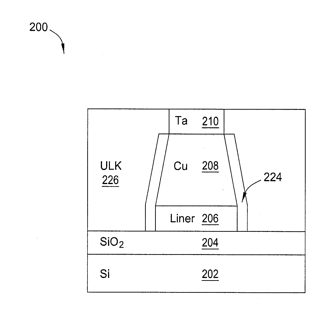
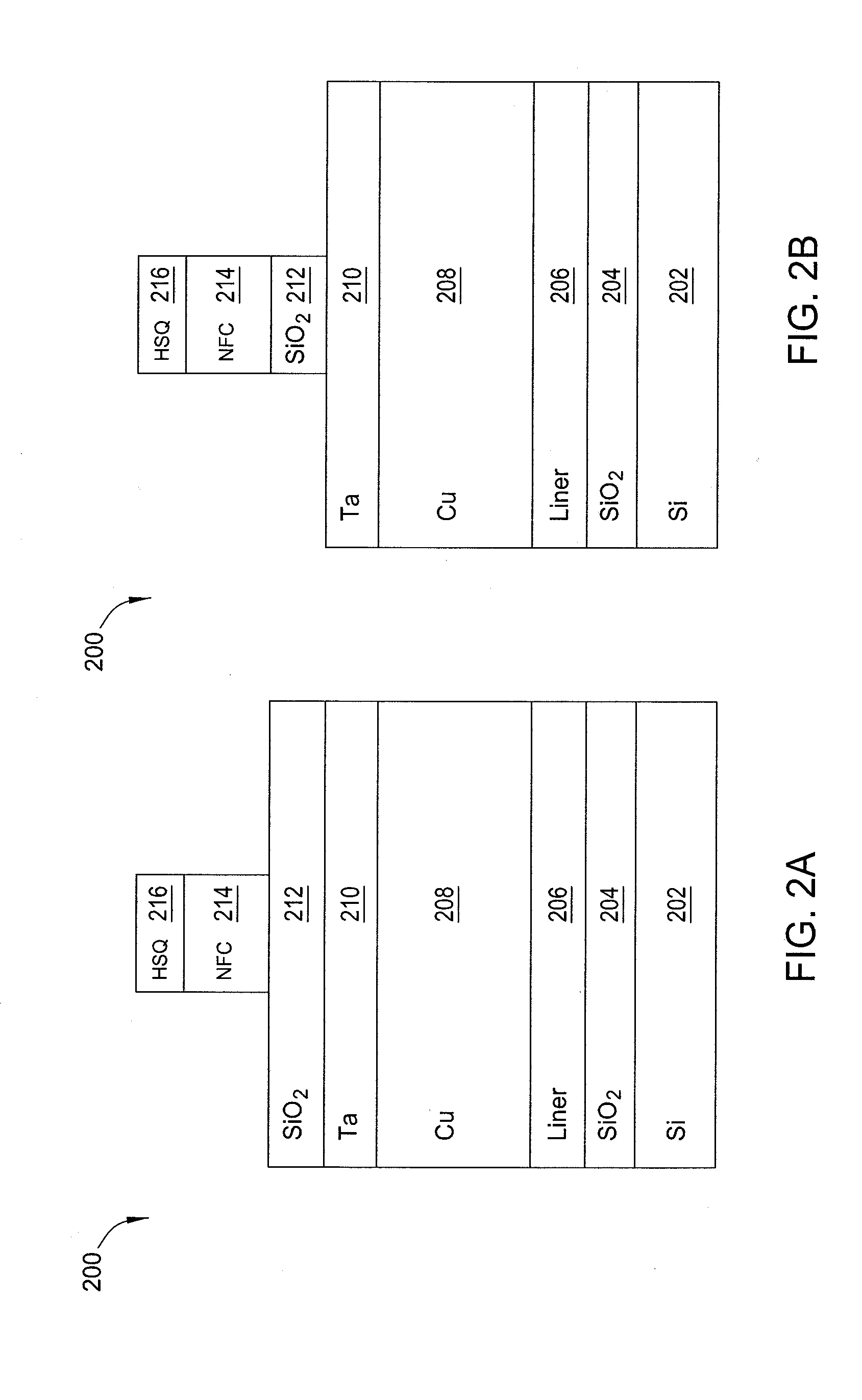
[0011]In one embodiment, the invention is a method and apparatus for heavy metal patterning using a sputter etch process. Embodiments of the invention pattern fine metal lines on an insulating layer of an integrated circuit via a subtractive process (i.e., a process that creates a desired structure by removing material rather than by adding material). In a particular embodiment, the subtractive process uses chlorine and fluorine etch chemistry in a two-step process to control the patterning of hard masks on copper containing conductive metal. In particular, the disclosed process allows for easier control of the hard mask profile during subtractive copper and copper alloy etching, as well as easier control of the copper patterning.

[0012]FIGS. 2A-2J are schematic diagrams illustrating various stages of fabrication of a complementary metal-oxide-semiconductor (CMOS) device 200, according to embodiments of the present invention. As such, FIGS. 2A-2J also collectively serve as a flow diagra


PUM


Abstract

A method for fabricating one or more conductive lines in an integrated circuit includes providing a layer of copper containing conductive metal in a multi-layer structure fabricated upon a wafer, providing a first hard mask layer over the layer of copper containing conductive metal, performing a first sputter etch of first hard mask layer using a chlorine-based plasma or a sulfur fluoride-based plasma, and performing a second sputter etch of first hard mask layer using a second plasma, wherein a portion of the layer of copper containing conductive metal residing below a portion of the first hard mask layer that remains after the second sputter etch forms the one or more conductive lines. In one embodiment, the second plasma is a fluorocarbon-based plasma.

Description


Claims


Application Information

Patent Timeline
Owner APPLIED MATERIALS INC
Why Eureka
Try Eureka