Self-aligned trench isolation method and semiconductor device fabricated using the same

Active Publication Date: 2005-10-11
SAMSUNG ELECTRONICS CO LTD
View PDF8 Cites 2 Cited by
  • Summary
  • Abstract
  • Description
  • Claims
  • Application Information

AI Technical Summary

Benefits of technology

[0024]Some embodiments of the invention prevent two different gate conductive layers from overlapping with each other in a border region between the cell array region an

Problems solved by technology

Accordingly, there may be some limitations in applying the self-aligned trench isolation technique to the flash memory devices.
Consequently

Method used


Image

  • Self-aligned trench isolation method and semiconductor device fabricated using the same
  • Self-aligned trench isolation method and semiconductor device fabricated using the same
  • Self-aligned trench isolation method and semiconductor device fabricated using the same

Examples


Embodiment Construction

[0028]Embodiments of the invention will now be described more fully hereinafter with reference to the accompanying drawings, in which preferred embodiments of the invention are shown. This invention may, however, be embodied in many different forms and should not be construed as limited to the embodiments set forth herein. Rather, these embodiments are provided so that this disclosure will be through and complete, and will fully convey the scope of the invention to those skilled in the art. In the drawings, the thickness of the layers and regions are exaggerated for clarity. Like numbers refer to like elements throughout the specification.

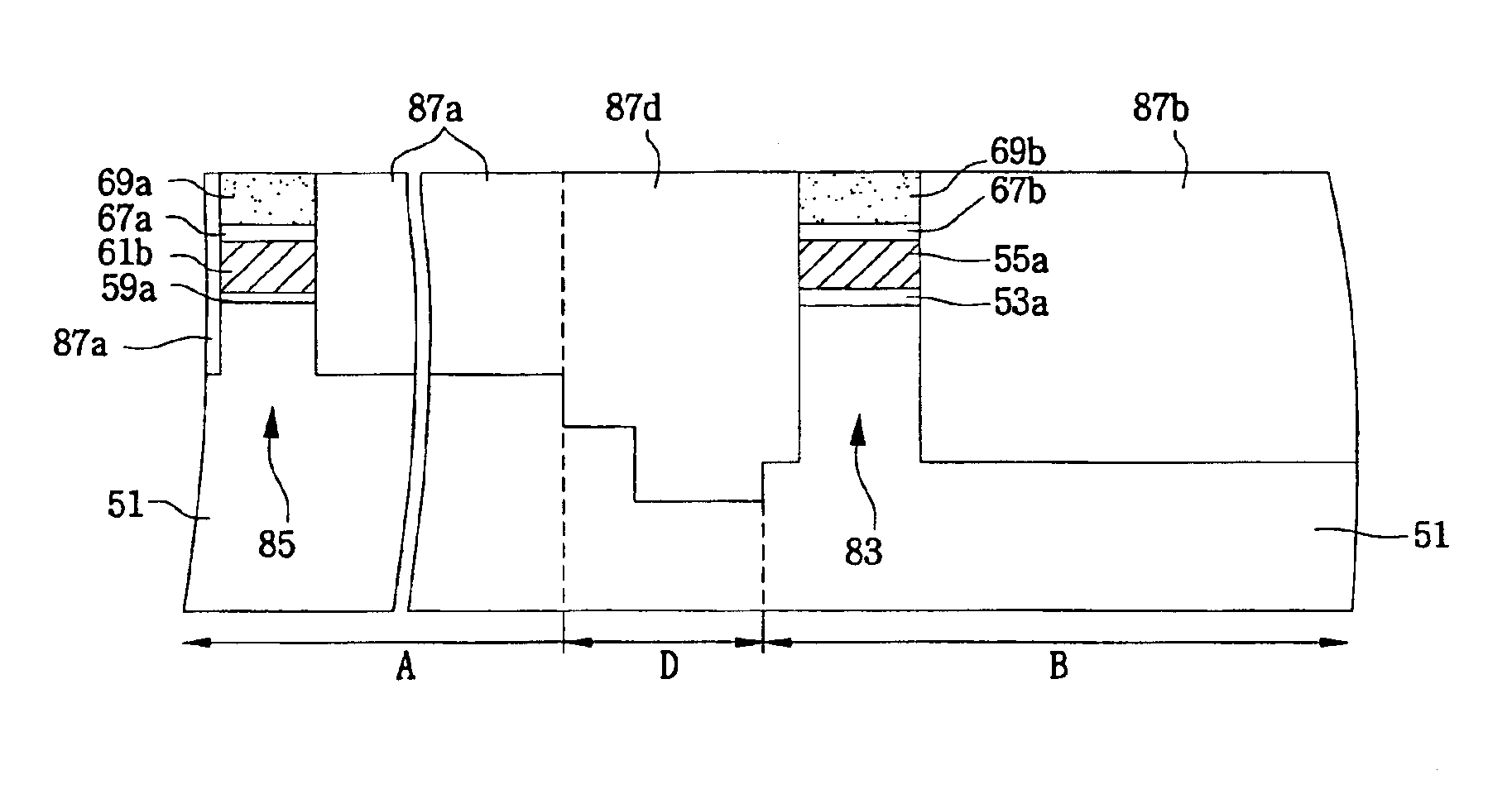
[0029]FIGS. 9 to 15 are cross-sectional diagrams illustrating self-aligned trench isolation methods according to some embodiments of the invention and semiconductor memory devices fabricated using the same.

[0030]Referring to FIG. 9, a first gate insulating layer, a first lower gate conductive layer and a gate etching stopper layer are sequentially for


PUM


Abstract

A method according to some embodiments of the invention includes forming a first gate pattern on a first region of a semiconductor substrate. The first gate pattern is formed to have a first gate insulating layer pattern, a first lower gate conductive layer pattern and a gate etching stopper layer pattern which are sequentially stacked. A second gate pattern is formed on a second region spaced apart from the first region to define a border region between the first and second regions. The second gate pattern is formed to have a second gate insulating layer pattern and a second lower gate conductive layer pattern, which are sequentially stacked. Thus, some embodiments may prevent two different gate conductive layers from overlapping with each other in the border region. Accordingly, semiconductor memory devices according to some embodiments of the invention do not have undesired active regions formed in the border region.

Description


Claims


Application Information

Patent Timeline
Owner SAMSUNG ELECTRONICS CO LTD
Why Eureka
Try Eureka