Substrate processing apparatus and substrate processing method
a processing apparatus and substrate technology, applied in the direction of photomechanical apparatus, instruments, transportation and packaging, etc., can solve the problems of affecting the formation of precise circuit patterns, affecting the yield of substrates, so as to prevent fine impurities at molecular level
- Summary
- Abstract
- Description
- Claims
- Application Information
AI Technical Summary
Benefits of technology
Problems solved by technology
Method used
Image

Examples
first embodiment
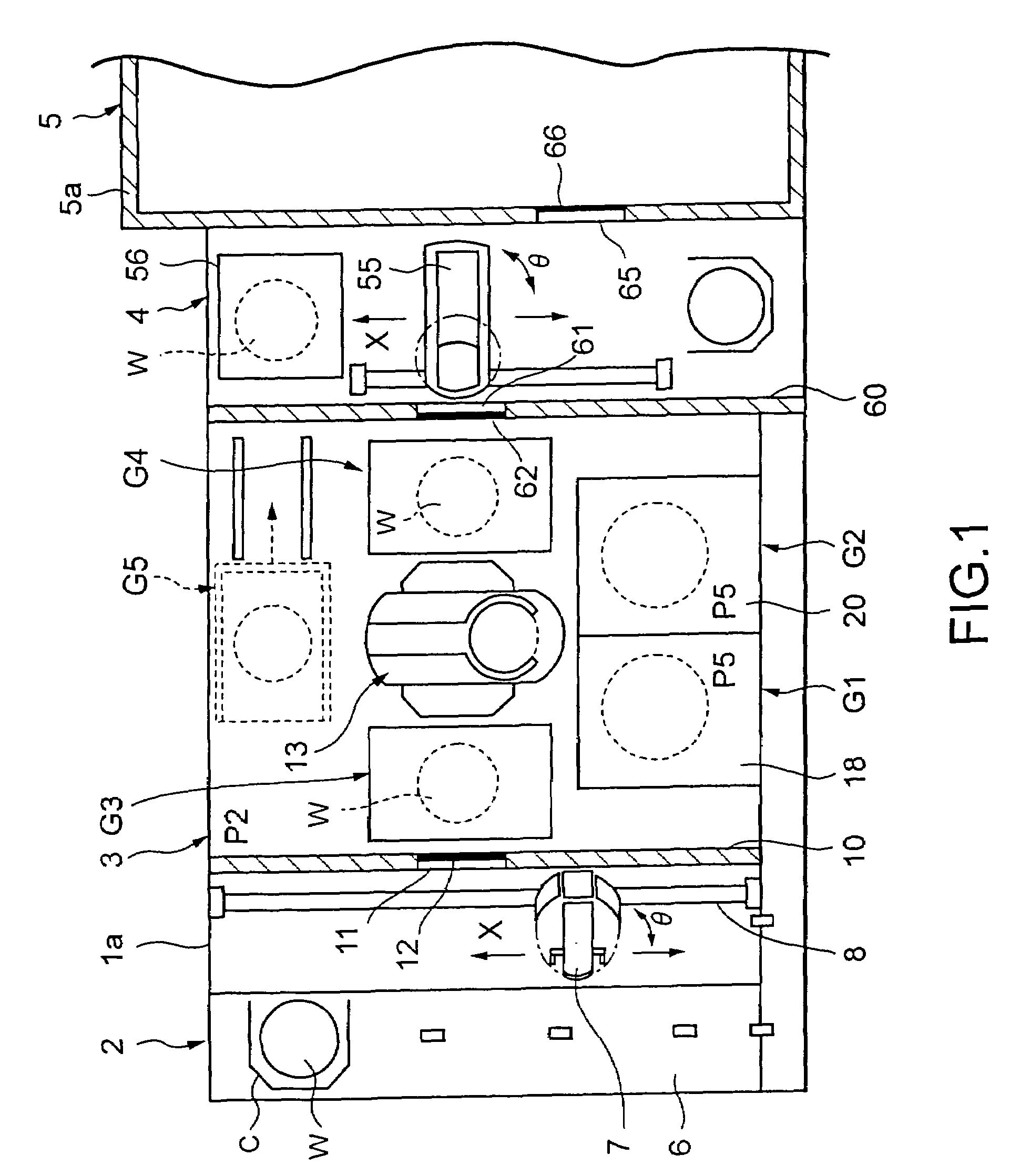
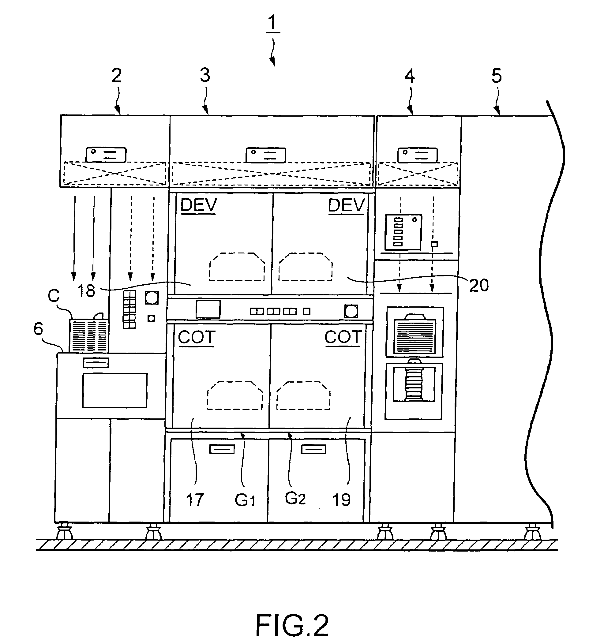
[0113]FIG. 1 is a plane view of a coating and developing processing system (substrate processing apparatus) 1 according to this embodiment, FIG. 2 is a front view of the coating and developing processing system 1, and FIG. 3 is a rear view of the coating and developing processing system 1.
[0114]The coating and developing processing system 1, as shown in FIG. 1, has a structure in which a cassette station 2 as a loader / unloader section, for carrying, for example, 25 wafers W in a cassette into / out of the coating and developing processing system 1 from / to the outside and for carrying the wafer W into / out of a cassette C, a processing station 3 as a processing section, in which various processing units for performing predetermined processing for wafers W one by one in a process of a coating and developing processing are disposed in multiple tiers, and an interface section 4 which receives and sends the wafer W from / to an aligner 5 provided next to the coating and developing proc
second embodiment
[0149]FIG. 7 is a plane view of a coating and developing processing system 101 according to the second embodiment, and FIG. 8 is a front view of the coating and developing processing system 101.
[0150]The coating and developing processing system 101, as shown in FIG. 7, has a structure in which a cassette station 102 for carrying, for example, 25 wafers W in a cassette into / out of the coating and developing processing system 101 from / to the outside and carrying the wafer W into / out of a cassette C, a processing station 103 as a processing section, in which various processing units are disposed in multiple tiers for performing predetermined processing for the wafers W one by one in a process of the coating and developing processing, and an interface section 104 for receiveing and sending the wafer W from / to an aligner 105 provided next to the coating and developing processing system 101 are integrally connected in its casing 101a.
[0151]In the cassette station 102, a plurality of
third embodiment
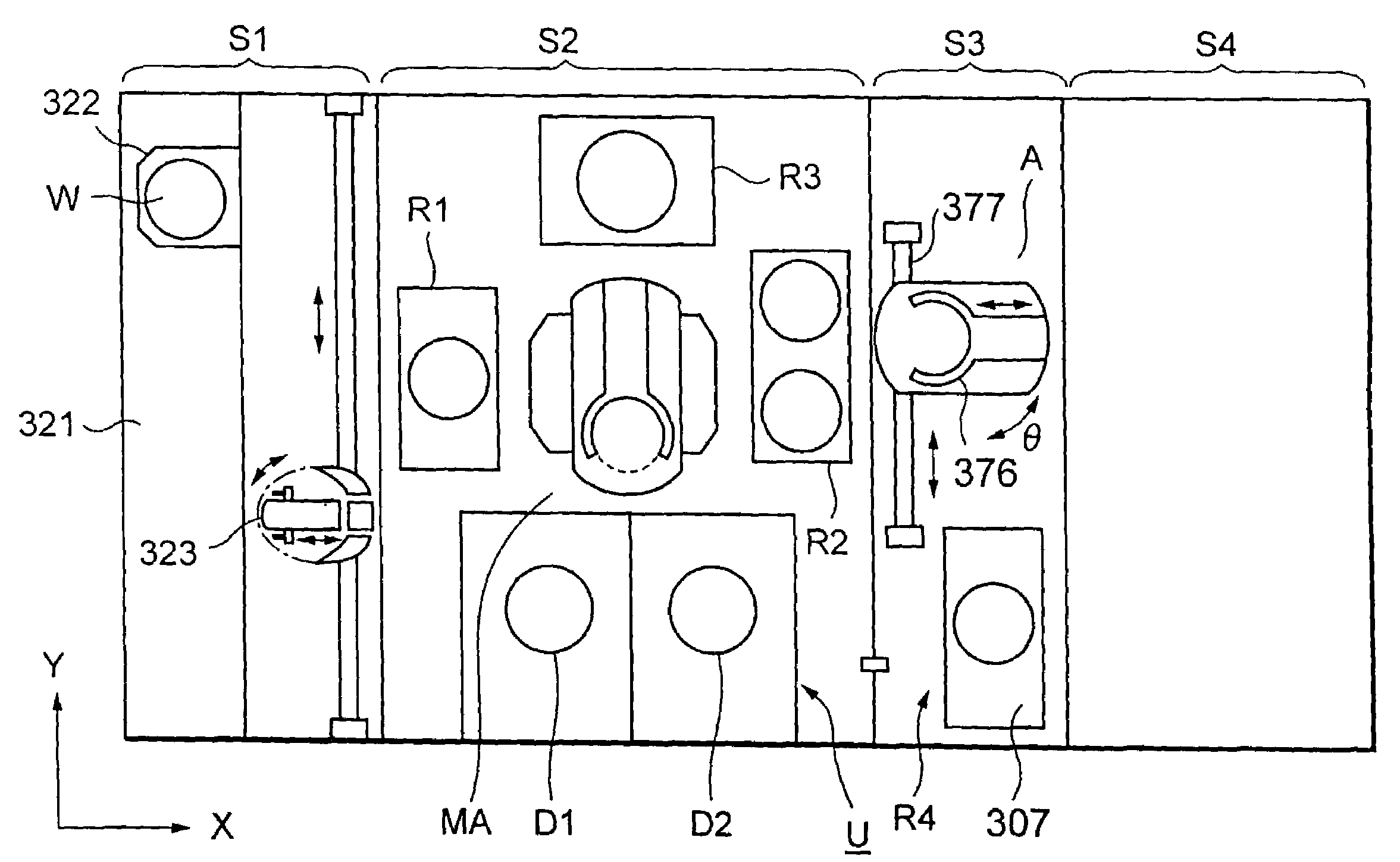
[0192]Next, the third embodiment of the present invention will be explained.
[0193]FIG. 16 is a plane view of a substrate processing apparatus according to this embodiment.
[0194]An apparatus 200 in FIG. 16 includes an interface section 202 in which a chamber 201 for temporarily holding the wafer W delivered from a processing station 3 and to be transferred to the aligner 5, in the interface section 4 in the system as shown in FIG. 1, for example.
[0195]An atmosphere inside the chamber 201 is controlled by an atmosphere controller 203.
[0196]For example, the atmosphere controller 203 reduces the pressure inside the chamber 201. Incidentally, the atmosphere controller 203 may be structured to supply an inert gas into the chamber 201 and to supply dry air into the chamber 201.
[0197]Further, the chamber 201 includes a purge room 204 which temporarily holds the wafer W introduced into the chamber to purge it, a buffer room 205 which holds the wafer W, and a transfer device 206 which is dispose
PUM
| Property | Measurement | Unit |
|---|---|---|
| Temperature | aaaaa | aaaaa |
| Area | aaaaa | aaaaa |
| Humidity | aaaaa | aaaaa |
Abstract
Description
Claims
Application Information
 - R&D Engineer
- R&D Manager
- IP Professional
- Industry Leading Data Capabilities
- Powerful AI technology
- Patent DNA Extraction
Browse by: Latest US Patents, China's latest patents, Technical Efficacy Thesaurus, Application Domain, Technology Topic.
© 2024 PatSnap. All rights reserved.Legal|Privacy policy|Modern Slavery Act Transparency Statement|Sitemap