Transparent conducting thin film and preparation method thereof
A technology of transparent conductive film and transparent substrate, applied in the field of electronics, can solve the problems of low square resistance, graphene film cannot have high visible light transmittance at the same time, etc., achieve low square resistance, high visible light transmittance, reduce cost effect
- Summary
- Abstract
- Description
- Claims
- Application Information
AI Technical Summary
Problems solved by technology
Method used
Image

Examples
Embodiment 1
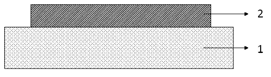
[0045] Complete the preparation of the transparent conductive film 2 through the following specific steps:
[0046] 1) cleaning the transparent substrate 1 of the glass, and drying it with dry nitrogen after cleaning;
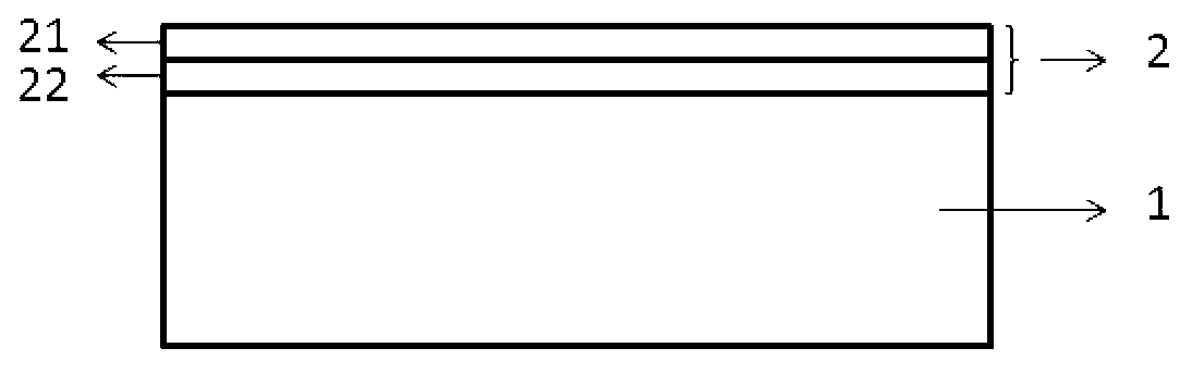
[0047] 2) A silver nanowire layer 21 is formed on the transparent substrate 1 by drop coating, the silver nanowire has a diameter of 40 nm and a length of 100 μm, and its density on the transparent substrate 1 is 0.005 mg / cm 2 ;
[0048] 3) adopt chemical vapor deposition (CVD) to form graphene sheet, and this graphene sheet is single-layer graphene;
[0049] 4) transfer the graphene sheet to the silver nanowire layer 21 by a dry method to form a graphene sheet 22, thereby preparing a composite layer consisting of the graphene sheet 22 and the silver nanowire layer 21 on the transparent substrate 1 transparent conductive film 2.
Embodiment 2
[0051] Complete the preparation of the transparent conductive film 2 through the following specific steps:
[0052] 1) Clean the flexible transparent substrate 1 of polyethylene terephthalate (PET), and dry it with dry nitrogen after cleaning;
[0053] 2) A silver nanowire layer 21 is formed on the transparent substrate 1 by scraping, the silver nanowire has a diameter of 60 nm and a length of 200 μm, and its density on the transparent substrate 1 is 0.0015 mg / cm 2 ;
[0054] 3) Graphene sheets are formed by graphene oxide after reduction, and the graphene sheets are double-layer graphene;
[0055] 4) Form a graphene sheet 22 on the silver nanowire layer 21 by spin coating, thereby preparing a transparent conductive film made of a combination layer of the graphene sheet 22 and the silver nanowire layer 21 on the transparent substrate 1 2.
Embodiment 3
[0057]Complete the preparation of the transparent conductive film 2 through the following specific steps:
[0058] 1) Clean the flexible transparent substrate 1 of polyethylene naphthalate (PEN), and dry it with dry nitrogen after cleaning;
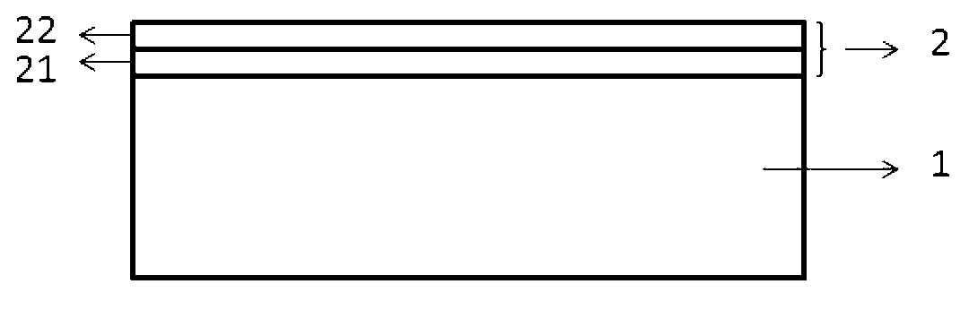
[0059] 2) adopt chemical vapor deposition (CVD) to form graphene sheet, and this graphene sheet is bilayer graphene;
[0060] 3) transfer the graphene sheet to the transparent substrate 1 by a wet method to form a graphene sheet 22;
[0061] 4) A silver nanowire layer 21 is formed on the graphene sheet 22 by spraying, the silver nanowire has a diameter of 60 nm and a length of 80 μm, and its density on the transparent substrate 1 is 0.005 mg / cm 2 , so that a transparent conductive film 2 composed of a combined layer of graphene sheet layer 22 and silver nanowire layer 21 is prepared on the transparent substrate 1 .
PUM
| Property | Measurement | Unit |
|---|---|---|
| Diameter | aaaaa | aaaaa |
| Length | aaaaa | aaaaa |
| Diameter | aaaaa | aaaaa |
Abstract
Description
Claims
Application Information
 - R&D Engineer
- R&D Manager
- IP Professional
- Industry Leading Data Capabilities
- Powerful AI technology
- Patent DNA Extraction
Browse by: Latest US Patents, China's latest patents, Technical Efficacy Thesaurus, Application Domain, Technology Topic.
© 2024 PatSnap. All rights reserved.Legal|Privacy policy|Modern Slavery Act Transparency Statement|Sitemap