Top gate structure metallic oxide thin film transistor for improving device uniformity and manufacture method thereof
A technology of oxide thin film and oxide film layer, which is applied in the direction of transistor, semiconductor/solid-state device manufacturing, semiconductor device, etc., can solve the problems of insufficient uniformity and stability, and achieve improved uniformity, high performance, and reduced contact resistance Effect
- Summary
- Abstract
- Description
- Claims
- Application Information
AI Technical Summary
Problems solved by technology
Method used
Image

Examples
Example Embodiment
[0050] Example 1
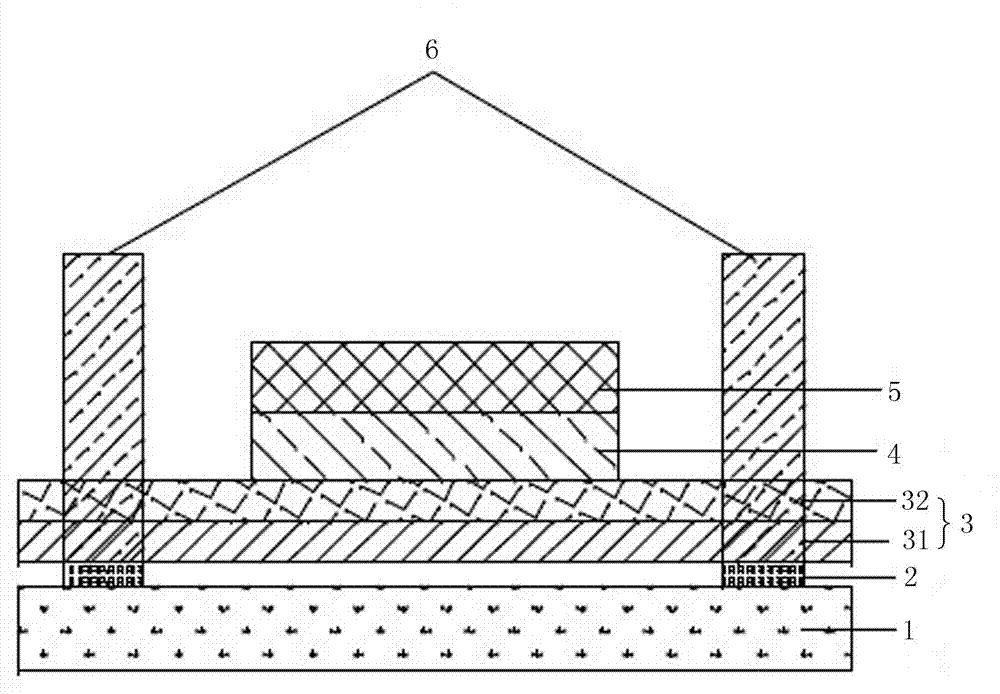
[0051] (1) Sputter 20nm oxygen-deficient IGZO (made in single-component Ar atmosphere) on alkali-free glass, and then sputter 5nm oxygen-rich IGZO (made in single-component oxygen atmosphere) with the same target; then wet method Etching and patterning IGZO;
[0052] (2) Annealing in a dry oxygen atmosphere and 350℃ for one hour;
[0053] (3) Sputtering 20nm silicon dioxide and 300nm silicon nitride as an insulating layer on the composite active layer;
[0054] (4) Anneal in air and 200℃ for one hour;
[0055] (5) Sputtering 100nm metal molybdenum as the gate electrode;
[0056] (6) Sputtering 100nm metal molybdenum as source / drain electrodes.
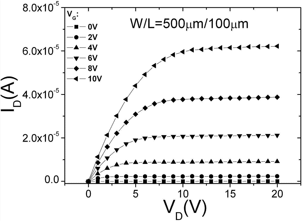
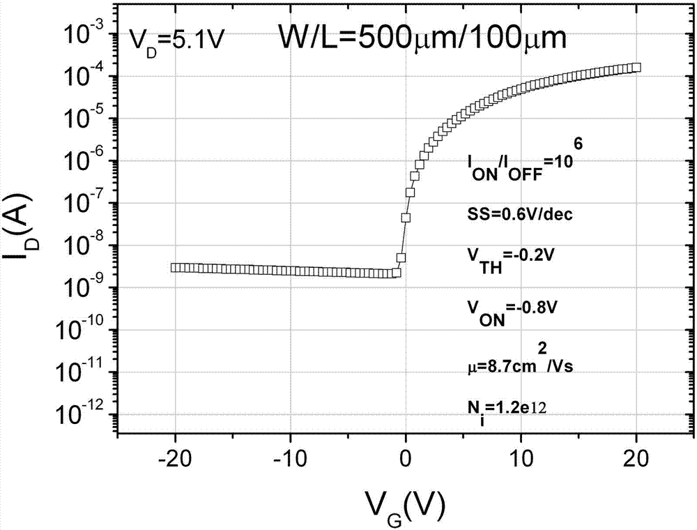
[0057] In addition, in this embodiment 1, please refer to the output characteristic curve figure 2 , Please refer to the transfer characteristic curve image 3 .
Example Embodiment
[0058] Example 2
[0059] In this implementation, thin film transistors were fabricated according to methods and conditions similar to those of Example 1. The difference is that (2) in Example 1 was annealed in a dry oxygen atmosphere and a temperature of 300° C. for one hour.
[0060] In addition, in the second embodiment, please refer to the output characteristic curve Figure 4 , Please refer to the transfer characteristic curve Figure 5 .
Example Embodiment
[0061] Example 3
[0062] In this implementation, thin film transistors were fabricated according to methods and conditions similar to those of Example 1. The difference is that the steps for adding and changing are as follows:
[0063] (1) On the alkali-free ITO glass, wet etch and pattern ITO to obtain the auxiliary electrode of the active layer;
[0064] (2) After IGZO is patterned, it is annealed in a dry oxygen atmosphere at 300℃ for one hour;
[0065] (3) During the IGZO patterning process, in the active layer auxiliary electrode area, IGZO is opened.
[0066] In addition, in the third embodiment, please refer to the output characteristic curve Image 6 , Please refer to the transfer characteristic curve Figure 7 .
[0067] Table 1: Comparison of characteristics of various examples
[0068] .
[0069] From the results in Table 1, it can be seen that fabricating auxiliary electrodes under the active layer can effectively improve the uniformity of thin film transistors; improve device
PUM
 Abstract
Description
Claims
Application Information
 - R&D Engineer
- R&D Manager
- IP Professional
- Industry Leading Data Capabilities
- Powerful AI technology
- Patent DNA Extraction
Browse by: Latest US Patents, China's latest patents, Technical Efficacy Thesaurus, Application Domain, Technology Topic.
© 2024 PatSnap. All rights reserved.Legal|Privacy policy|Modern Slavery Act Transparency Statement|Sitemap