Formation method of semiconductor structure

A semiconductor and wet etching technology, used in semiconductor devices, semiconductor/solid-state device manufacturing, electrical components, etc., can solve problems such as large leakage current and large parasitic capacitance, and achieve the purpose of reducing leakage current, reducing leakage current, increasing The effect of oxidation rate

Inactive Publication Date: 2017-07-14
SEMICON MFG INT (SHANGHAI) CORP +1
View PDF4 Cites 0 Cited by
  • Summary
  • Abstract
  • Description
  • Claims
  • Application Information

AI Technical Summary

Benefits of technology

This new technology allows for better control over how well metal layers used within electronic devices (such as transistors) work by removing certain parts or materials from their surfaces without affecting other components like wires that connect them together. By doing this, it improves efficiency and performance of these electronics while reducing its size and cost-effectiveness compared to previous methods.

Problems solved by technology

This patented technical problem addressed in this patents relates to improving the efficiency at controlling power consumption while reducing interference from unwanted signals caused by external sources such as noise or other factors that may be present during operation.

Method used


Image

  • Formation method of semiconductor structure
  • Formation method of semiconductor structure
  • Formation method of semiconductor structure

Examples


Embodiment Construction

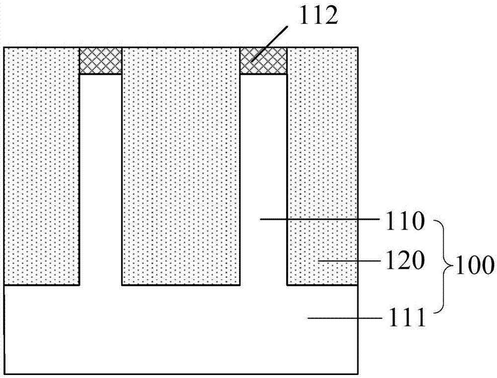
[0044] There are many problems in the existing methods for forming semiconductor structures, including: the shortcoming of large leakage current of the formed transistors.

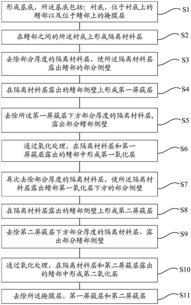
[0045] The fin of the fin field effect transistor formed in the prior art is formed by etching the substrate, and a transistor is formed on the fin, and the fin is in direct contact with the substrate. After the transistor is formed, the trench Carriers in the channel easily enter the substrate, forming a leakage current. Therefore, the leakage current of the transistor formed in the prior art is relatively large.

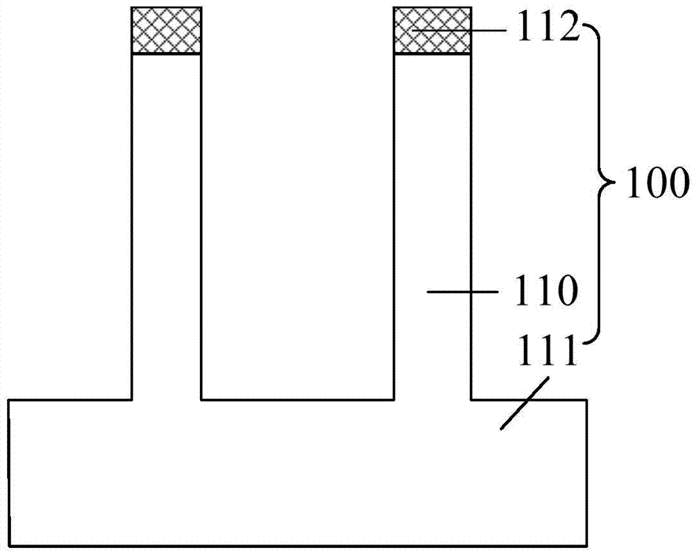
[0046] In order to solve the above technical problem, the present invention provides a method for forming a semiconductor structure, including: forming a base, the base includes: a substrate, a fin on the substrate, and a mask layer on the fin; An isolation material layer is formed on the substrate between the fins; at least one oxide layer is formed in the fins through at least one oxidation ste


PUM

PropertyMeasurementUnit
Thicknessaaaaaaaaaa
Thicknessaaaaaaaaaa
Thicknessaaaaaaaaaa

Abstract

The invention provides a formation method of a semiconductor structure. The formation method comprises the steps of forming a base, wherein the base comprises a substrate, fin parts and mask layers, wherein the fin parts are arranged on the substrate, and the mask layers are arranged on the fin parts; forming an isolation material layer on the substrate between the fin parts; and forming at least one oxide layer in the fin parts by oxidization step for at least one time, wherein the oxidization step comprises the steps of removing a partial thickness of the isolation material layer so that a part of a side wall of each fin part is exposed out of the isolation material layer; forming a shielding layer on the isolation material layer where the side wall of the fin part is exposed; removing a partial thickness of the isolation material layer below the shielding layer to expose a part of the side wall of the fin part; forming the oxide layer in the fin parts exposed out of the isolation material layer and the shielding layer by oxidization processing; and removing the mask layers and the shielding layer which is used in the oxidization step, wherein the isolation between the fin parts and the substrate can be achieved by the oxidization layer, and the oxidization layer can be used for reducing leakage currents of transistors after the transistors are formed in the fin parts.

Description


Claims


Application Information

Patent Timeline
Owner SEMICON MFG INT (SHANGHAI) CORP
Why Eureka
Try Eureka