GaN compatible driving circuit

A technology of compatible drive and circuit, which is applied in the field of GaN compatible drive circuit, can solve the problems of not being able to drive GaN devices without integrated drive, low on-resistance and gate charge, and demanding drive performance, achieving convenient iteration, high reliability, low cost effect

Pending Publication Date: 2021-11-26
SHENZHEN FAHOLD ELECTRONICS CO LTD
View PDF0 Cites 1 Cited by
  • Summary
  • Abstract
  • Description
  • Claims
  • Application Information

AI Technical Summary

Problems solved by technology

[0002] Gallium nitride (GaN) power devices have been rapidly developed in high switching speed and high power density applications. GaN has lower on-resistance and gate charge than traditional silicon-based MOSFETs, especially when working at high switching frequencies. The application in GaN devices with a series structure makes its driving performan

Method used


Image

  • GaN compatible driving circuit
  • GaN compatible driving circuit
  • GaN compatible driving circuit

Examples


Embodiment 1

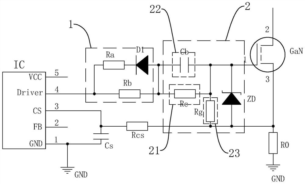
[0038] refer to figure 1 , the GaN compatible drive circuit includes a drive chip IC, a MOS drive module 1 and a GaN drive compatible module 2, the drive terminal of the drive chip IC is connected to the input terminal of the MOS drive module 1, the GaN drive compatible module 2 includes a voltage limiting unit 21, an acceleration unit 22 and a voltage dividing unit 23, the input end of the voltage limiting unit 21 is connected to the output end of the MOS drive module 1, the output end of the voltage limiting unit 21 is connected to the input end of the voltage dividing unit 23, and the gate of the N-type field effect transistor, The output end of the voltage dividing unit 23 is connected to the source of the N-type field effect transistor and the driving chip IC, and the accelerating unit 22 and the voltage limiting unit 21 are connected in parallel.

[0039] In this embodiment, the MOS drive module 1 includes a first resistor Ra, a diode D1 and a second resistor Rb, one end of

Embodiment 2

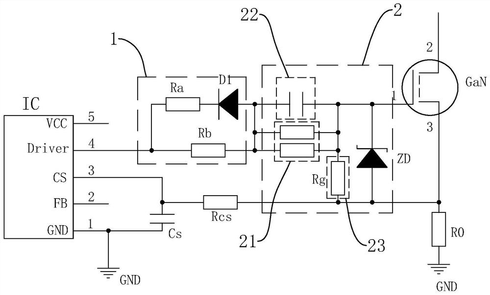
[0053] refer to figure 2 , The difference between this embodiment and Embodiment 1 is that there are multiple voltage limiting resistors, and multiple voltage limiting resistors are connected in series or in parallel.

Embodiment 3

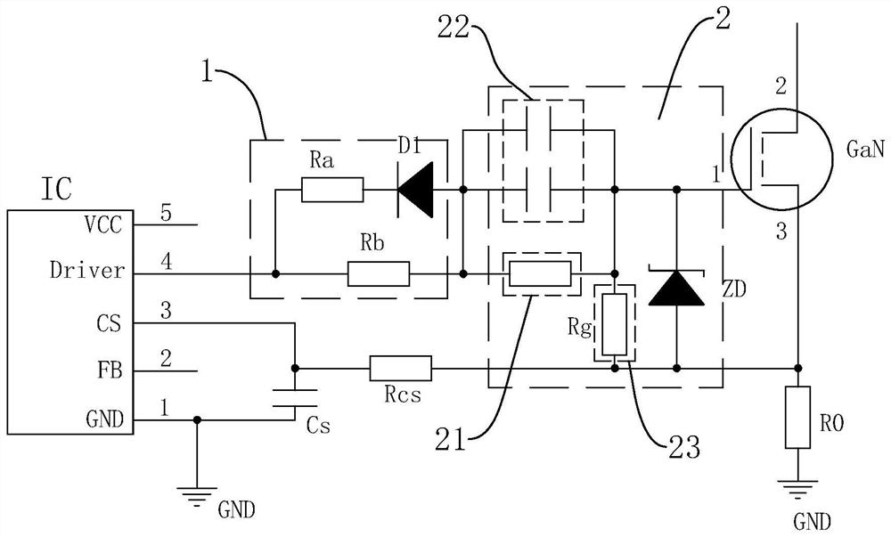
[0055] refer to image 3 , The difference between this embodiment and Embodiment 1 is that there are multiple speed-up capacitors Cb, and multiple speed-up capacitors Cb are connected in parallel.


PUM

PropertyMeasurementUnit
Regulator valueaaaaaaaaaa

Abstract

The invention discloses a GaN compatible driving circuit, and belongs to the technical field of semiconductor devices, the GaN compatible driving circuit comprises a driving chip IC, an MOS driving module and a GaN driving compatible module, the driving end of the driving chip IC is connected with the input end of the MOS driving module, the GaN driving compatible module comprises a voltage limiting unit, an acceleration unit and a voltage dividing unit, the input end of the voltage limiting unit is connected with the output end of the MOS driving module, the output end of the voltage limiting unit is connected with the input end of the voltage dividing unit and the grid electrode of the N-type field effect transistor, the output end of the voltage dividing unit is connected with the source electrode of the N-type field effect transistor and the driving chip IC, and the acceleration unit is connected with the voltage limiting unit in parallel. The method has the effect that the GaN and the silicon-based MOSFET can be driven in a compatible mode.

Description


Claims


Application Information

Patent Timeline
Owner SHENZHEN FAHOLD ELECTRONICS CO LTD
Why Eureka
Try Eureka