Multistage surface modification procedure of semiconducting nanoparticles for use in hybrid solar cells and printable electronics
a technology of semiconducting nanoparticles and printable electronics, which is applied in the direction of fatty acid chemical modification, non-metal conductors, conductors, etc., can solve the problems of reducing energy conversion efficiency and lifetime, reducing the efficiency of organic solar cells, and consuming a lot of manpower, so as to achieve the effect of effective use of solar cells and simple and reliable substitution of primary ligands by intermediate ligands
- Summary
- Abstract
- Description
- Claims
- Application Information
AI Technical Summary
Benefits of technology
Problems solved by technology
Method used
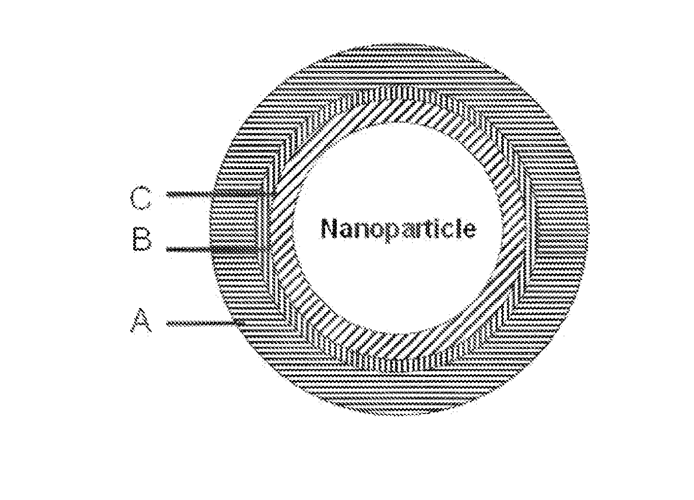
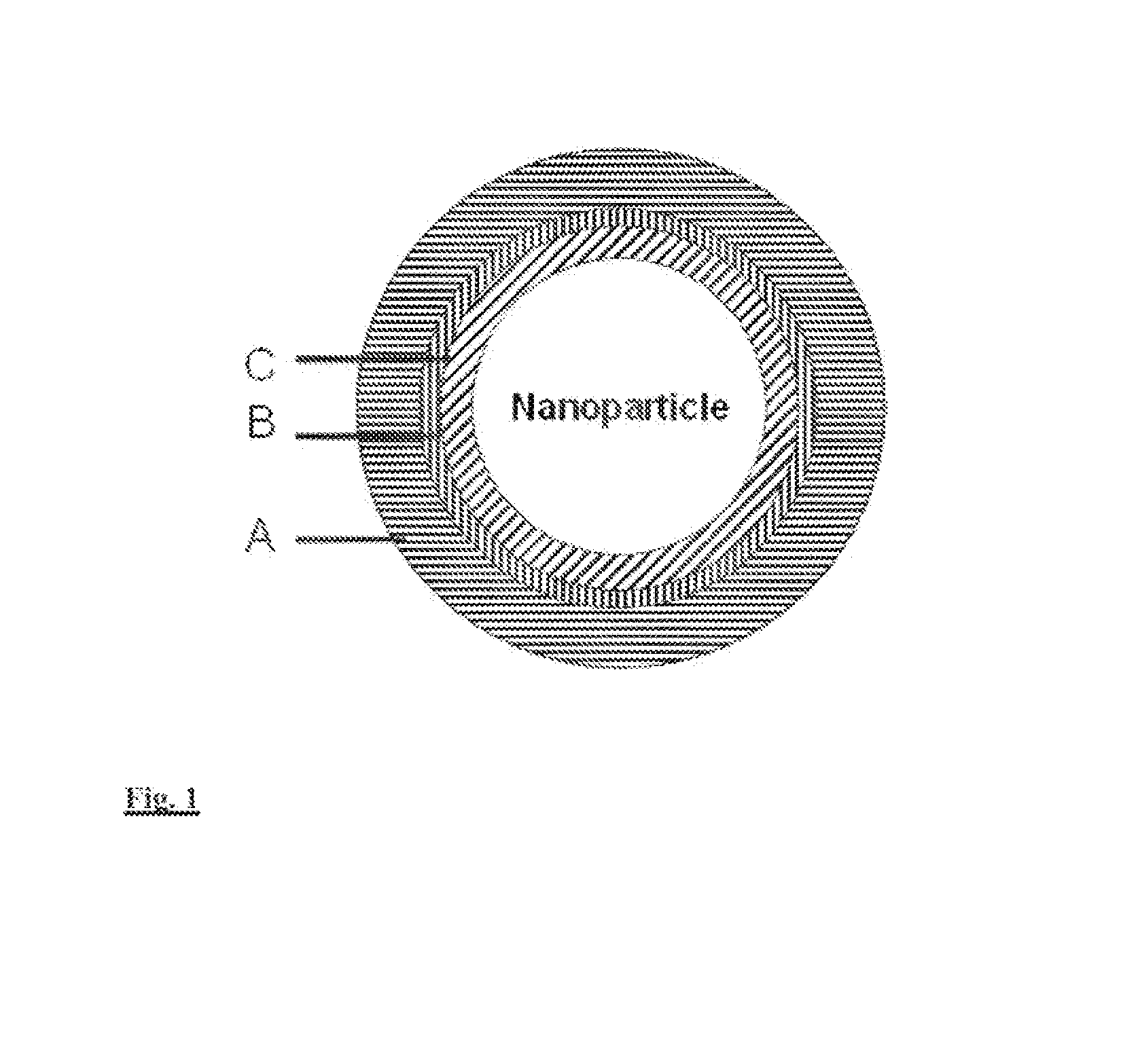
Image

Examples
example 1
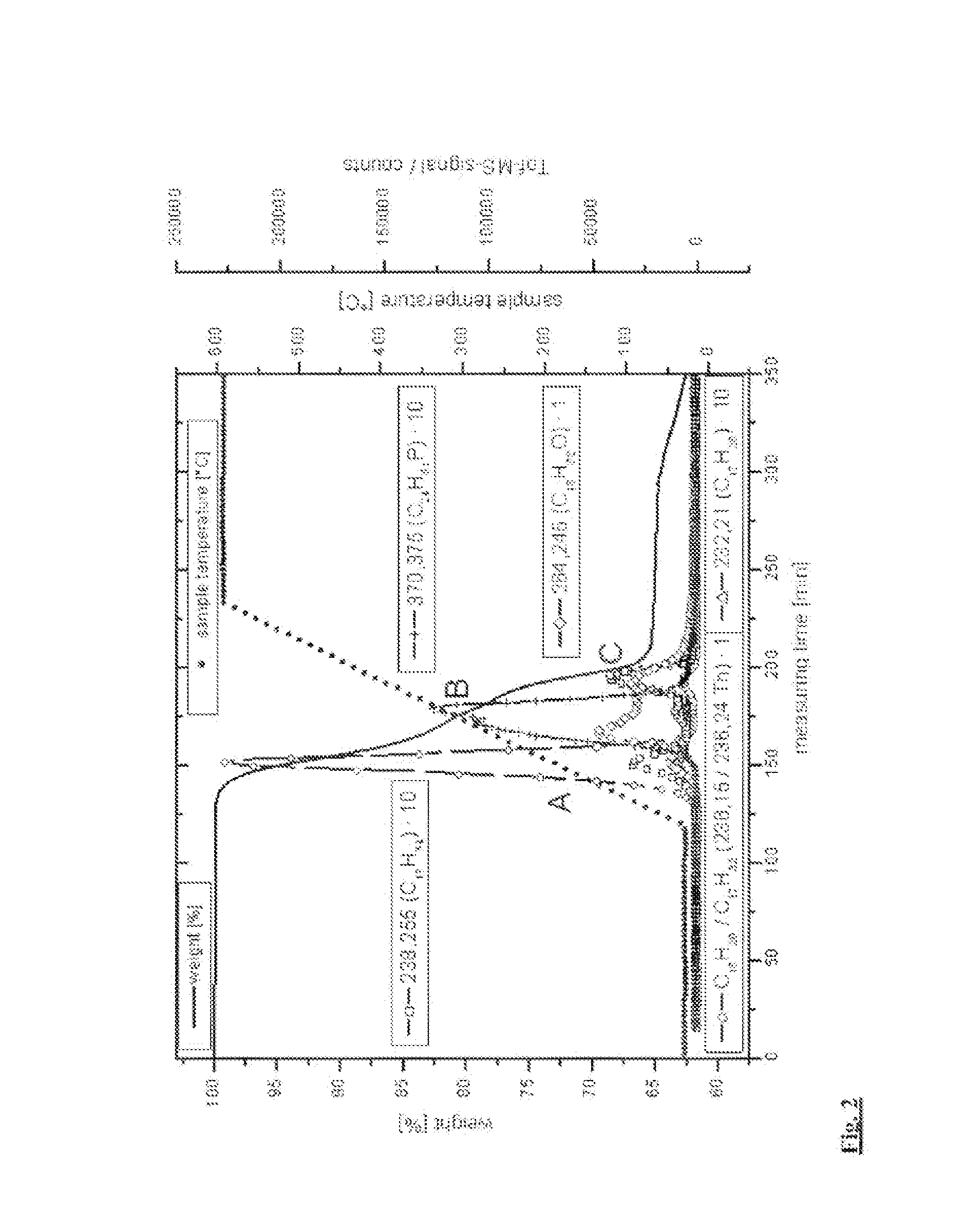
Thermo Gravimetric Analysis-Mass Spectrometry (TGA-MS) Measurement of CdSe Nanoparticle of Quantum Dot Shape (CdSe-QD) with Primary Ligand Trioctylphosphine (=TOP) and Oleic Acid (=OA)
[0103]Semiconducting nanopartieles CdSe-QD with primary ligand trioctylphosphine (=TOP) and oleic acid (=OA) were prepared according to the method of US2007 / 0132052A1
[0104]The TGA-MS measurements are performed with dried semiconducting nanoparticles under an inert atmosphere to prevent oxidation or other undesired reactions during the analysis. The amount of the dried sample should he at least 50 mg.
[0105]50 mg of dried sample were loaded onto a high-precision balance pan placed in a small electrically heated oven with thermocouple accurately measuring the internal oven temperature.
[0106]An inert gas preferably Ar or He and most preferably He with a flow rate of 80 ml / minute was flown into the overt for preferably at least two tours to purge away traces of oxygen and water out of the oven.
[0107]Then t
example 2
Preparation of CdSe-QD with Primary Ligand TOP and OA Using MeOH According to the Method of US2007 / 0132052A1 and Solar Cell Preparation
[0113]A—Washing of CdSe-QD with primary ligand TOP and OA using MeOH according to the method of US2007 / 0132052A1.
[0114]Above mentioned CdSe-QD with primary ligand TOP and OA were prepared and washed with MeOH according to the method of US2007 / 0132052A1.
[0115]Weight percentage distribution obtained alter TGA-MS Analysis according to the method of example 1 is shown is FIG. 3, column 2.
[0116]FIG. 4A shows a TEM Picture (made with TEM-FEI Tecnai 20 of CdSe nanoparticles after 3×MeOH washing.
[0117]B—Preparation of a solar cell using an ink comprising semiconductor nanoparticles of example 2-A
[0118]100 mg of the CdSe-QD with ligand TOP and OA of example 2-A were dispersed in 1 mL of the ink solvent (chlorobenzene) as the first stock solution. The 11 mg of a second semiconducting material (poly(3-hexylthiophene) or P3HT) were dispersed in 1 mL of the in
example 3
Washing of CdSe-QD with Primary Ligand TOP and OA Using MeOH and n-Hexane According to the Method of the Present Invention and Solar Cell Preparation
[0122]100 mg of the above mentioned CdSe-QD with primary ligand TOP and OA were precipitated by methanol according to the method of US2007 / 0132052A1. The semiconducting nanoparticles CdSe-QD were separated from the supernatant by centrifugation and dried with nitrogen gas. The dried semiconducting nanoparticles CdSe were redispersed in 1 ml n-Hexane with a concentration of 100 mg of CdSe nanoparticle per 1 mL of n-Hexane and stirred at room temperature for 12-24 hours. Subsequently 10 ml methanol were added into this dispersion to precipitate semiconducting nanoparticles and to remove further TOP and OA (ratio of dispersion solvent to washing agent 1:10). The precipitate was separated from supernatant by centrifugation. The semiconducting nanoparticles were dried with nitrogen gas and redispersed in 1 ml n-Hexane. Washing was repeated tw
PUM
 Abstract
Description
Claims
Application Information
 - R&D Engineer
- R&D Manager
- IP Professional
- Industry Leading Data Capabilities
- Powerful AI technology
- Patent DNA Extraction
Browse by: Latest US Patents, China's latest patents, Technical Efficacy Thesaurus, Application Domain, Technology Topic.
© 2024 PatSnap. All rights reserved.Legal|Privacy policy|Modern Slavery Act Transparency Statement|Sitemap