Single crystal pulling device, preparation method of single crystal silicon and single crystal silicon

A pulling device and monocrystalline silicon technology, applied in the direction of single crystal growth, single crystal growth, chemical instruments and methods, etc., can solve problems such as dislocation of single crystal silicon, improve crystal quality, reduce dislocation problems, clean work easy effect

Inactive Publication Date: 2019-04-02
XIAN ESWIN SILICON WAFER TECH CO LTD
View PDF3 Cites 2 Cited by
  • Summary
  • Abstract
  • Description
  • Claims
  • Application Information

AI Technical Summary

Benefits of technology

This technology prevents unwanted substances such as metal particles or other contaminants that may enter an apparatus used for growing monocrystalline materials (MCS) with high purity requirements. It achieves this through two main technical means - one involves controlling the movement of impurity-containing gases within the system itself while another approach focuses on reducing these harmful components' impacts upon the resulting material properties.

Problems solved by technology

The technical problem addressed in this patented technology relates to improving the efficiency at producing high-quality monocrystalline wafers from silicon materials used during production processes such as chemical vapor deposition or physical vapour phase epitaxy methods that require precise control over temperatures on specific areas within the wafer's surface layer. This can lead to issues like misalignment caused by thermal expansion differences between different parts of the waver due to changes in environmental factors such as humidity levels or other atmospheric conditions.

Method used


Image

  • Single crystal pulling device, preparation method of single crystal silicon and single crystal silicon
  • Single crystal pulling device, preparation method of single crystal silicon and single crystal silicon
  • Single crystal pulling device, preparation method of single crystal silicon and single crystal silicon

Examples


Embodiment Construction

[0035] In order to make the technical problems, technical solutions and advantages to be solved by the present invention clearer, the following will describe in detail with reference to the drawings and specific embodiments.

[0036] The terms "first", "second" and the like in the description and claims of the present invention are used to distinguish similar objects, and are not necessarily used to describe a specific order or sequence. It is to be understood that the data so used are interchangeable under appropriate circumstances such that the embodiments of the invention described herein are, for example, capable of practice in sequences other than those illustrated or described herein.

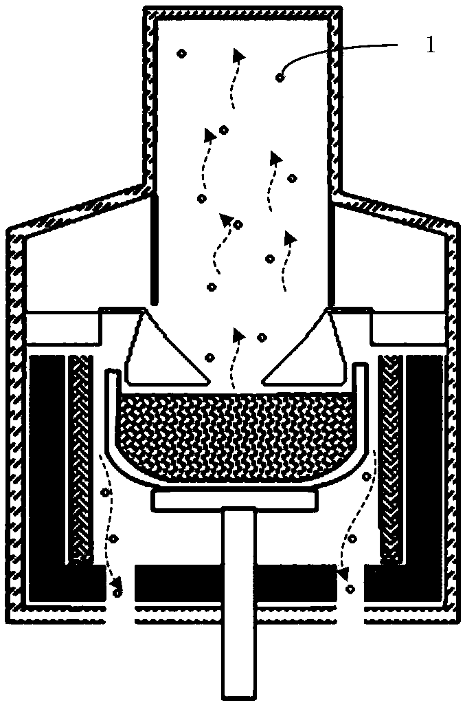
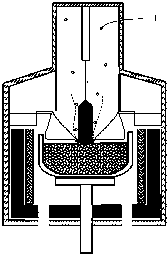
[0037] see figure 1 , in the process of manufacturing monocrystalline silicon, it is necessary to heat and melt the polysilicon placed in the crucible, and a large amount of impurities 1 (or called impurities) will be produced during the melting of polysilicon, and the impurities 1 can be ox


PUM


Abstract

Embodiments of the present invention provide a single crystal pulling device, a preparation method of single crystal silicon, and the single crystal silicon. The single crystal pulling device includesa housing, a melting member and a blocking member; the housing is provided with a receiving space, the receiving space includes at least a first chamber and a second chamber communicating with the first chamber, and the second chamber is located above the first chamber; the melting member is used for heating and melting polysilicon, and the melting member is fixed to the bottom of the first chamber; and the blocking member is located in the second chamber, and the blocking member is used for injecting an inert gas in a preset manner to prevent impurities generated by the polysilicon melting process from entering the upper chamber of the second chamber. With the single crystal pulling device disclosed by the embodiments of the invention, a large amount of impurities can be prevented from flowing into the upper chamber of the single crystal pulling device, thereby reducing the dislocation problem of a single crystal silicon rod caused by impurities, improving the crystal quality, and also facilitating the cleaning work of the receiving space.

Description


Claims


Application Information

Patent Timeline
Owner XIAN ESWIN SILICON WAFER TECH CO LTD
Why Eureka
Try Eureka