Hole transport material, QLED (Quantum dot Light-Emitting Diode) device and preparation method thereof
A hole-transporting material and hole-transporting layer technology, used in semiconductor/solid-state device manufacturing, electrical solid-state devices, semiconductor devices, etc. Transport performance, high hole transport ability, effect of improving stability
- Summary
- Abstract
- Description
- Claims
- Application Information
AI Technical Summary
Benefits of technology
Problems solved by technology
Method used
Image

Examples
preparation example Construction
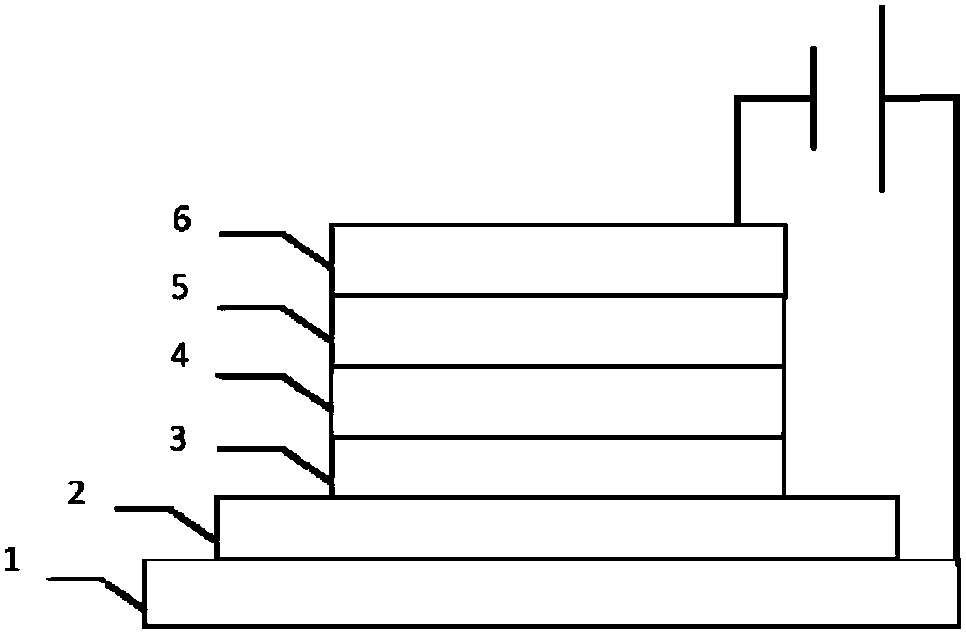
[0024] Finally, the present invention also provides a method for preparing a QLED device. The QLED device is a positive QLED device, and the QLED device includes a hole transport layer. The preparation method includes the following steps:
[0025] S01: providing a substrate, the substrate is provided with an anode;
[0026] S02: Provide a mixed colloid solution dispersed with graphyne and p-type metal oxide nanoparticles, deposit the mixed colloid solution on the anode, and dry to obtain a hole transport layer.
[0027] Alternatively, the QLED device is an inverted QLED device, and the QLED device includes a hole transport layer, and the preparation method includes the following steps:
[0028] T01: providing a substrate on which a quantum dot light-emitting layer is provided;
[0029] T02: providing a mixed colloidal solution dispersed with graphyne and p-type metal oxide nanoparticles, depositing the mixed colloidal solution on the quantum dot light-emitting layer, and drying
Embodiment 1
[0044] Taking molybdenum oxide and graphyne powder to prepare graphyne-doped hole transport layer as an example to introduce in detail:
[0045] First disperse molybdenum oxide with a particle size below 450nm in ultrapure water (the concentration of molybdenum oxide is 60-100mg / mL) and stir thoroughly, take graphyne powder with a particle size below 45nm, and evenly disperse it in the molybdenum oxide aqueous solution , wherein the mass ratio of graphyne to molybdenum oxide is (2-10): 100, stirred at a rate of 3000rpm / min for 30 minutes until the solution is completely uniform, and a graphyne-molybdenum oxide mixed colloid solution is obtained.
[0046] The graphyne-molybdenum oxide mixed colloid solution was spin-coated on the anode substrate, heated to 120° C. on a heating platform and kept for 15 minutes to form a hole transport layer.
Embodiment 2
[0048] Taking tungsten oxide and graphyne powder to prepare graphyne-doped hole transport layer as an example to introduce in detail:
[0049] First disperse tungsten oxide with a particle size below 450nm in ultrapure water (the concentration of tungsten oxide is 60-100mg / mL) and stir thoroughly, take graphyne powder with a particle size below 45nm, and disperse it evenly in an aqueous tungsten oxide solution , wherein the mass ratio of graphyne to tungsten oxide is (2-10): 100, stirring at a rate of 3000rpm / min for 30 minutes until the solution is completely uniform, and a graphyne-tungsten oxide mixed colloidal solution is obtained.
[0050] The graphyne-tungsten oxide mixed colloid solution was spin-coated on the anode substrate, heated to 120° C. on a heating platform and kept for 15 minutes to form a hole transport layer.
PUM
| Property | Measurement | Unit |
|---|---|---|
| Particle size | aaaaa | aaaaa |
Abstract
Description
Claims
Application Information
 - R&D Engineer
- R&D Manager
- IP Professional
- Industry Leading Data Capabilities
- Powerful AI technology
- Patent DNA Extraction
Browse by: Latest US Patents, China's latest patents, Technical Efficacy Thesaurus, Application Domain, Technology Topic.
© 2024 PatSnap. All rights reserved.Legal|Privacy policy|Modern Slavery Act Transparency Statement|Sitemap