Integrated circuit and manufacturing method thereof

A technology of integrated circuits and circuit substrates, which is applied in the direction of circuits, semiconductor/solid-state device manufacturing, and electrical components, etc., and can solve the problems of epoxy resin glue overflow, poor stability, and heavy workload when removing epoxy resin glue. To achieve the effect of enhanced stability

Active Publication Date: 2020-02-07
四川豪威尔信息科技有限公司
View PDF6 Cites 0 Cited by
  • Summary
  • Abstract
  • Description
  • Claims
  • Application Information

AI Technical Summary

Benefits of technology

This patented describes an improved process for integrally connecting electronic components onto a circuit substratum that improves their reliability during operation. It involves creating channels within the circuit baseplate without leaving any space around them or adding extra parts like bolts. A special type of adhesion agent called gamma-grove was developed which can be easily attached to the channel walls while still maintaining good contact with other areas. An insulating film filled with gelatin solder has openings along each side where there connects another component's terminals. After filling this gap with liquid epoxy glue, a curved squeegee device applies pressure to remove air from the interior of the chamber. Glucoid acid solution fills spaces above these openings and forms weakened bridges across the entirety of the internal structure.

Problems solved by technology

The technical problem addressed by this patented technology relating to an integration chip that has many parts connected together without damaging them during manufacturing processes like removing excessive adhesion material from the surface of each part before final assembly into a package.

Method used


Image

  • Integrated circuit and manufacturing method thereof
  • Integrated circuit and manufacturing method thereof
  • Integrated circuit and manufacturing method thereof

Examples


Embodiment Construction

[0029] The following will clearly and completely describe the technical solutions in the embodiments of the present invention with reference to the accompanying drawings in the embodiments of the present invention. Obviously, the described embodiments are only some, not all, embodiments of the present invention. Based on the embodiments of the present invention, all other embodiments obtained by persons of ordinary skill in the art without making creative efforts belong to the protection scope of the present invention.

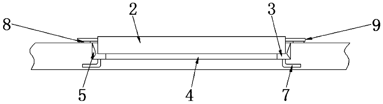
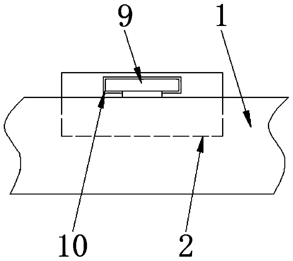
[0030] see Figure 1-4 , the embodiment of the present invention provides a technical solution: an integrated circuit, including a circuit substrate body 1, a chip 2 is bonded to the top of the circuit substrate body 1, a square groove 3 is opened on the top of the circuit substrate body 1, and the square groove 3 The inner surface and the outer surface of the chip 2 are bonded with epoxy resin, the inner surface of the square groove 3 is bonded to the outer surf


PUM

PropertyMeasurementUnit
Angleaaaaaaaaaa

Abstract

The invention discloses an integrated circuit, which comprises a circuit substrate body. A chip is bonded to the top of the circuit substrate body. A square groove is formed in the top of the circuitsubstrate body. The inner surface of the square groove is bonded to the outer surface of the chip. A glue absorption soft board is fixedly connected to the bottom of an inner cavity of the square groove, and the top of the glue absorption soft board is bonded to the bottom of the chip. The invention relates to the technical field of integrated circuits. According to the integrated circuit and themanufacturing method thereof, the square groove is arranged, the glue absorption soft board is arranged at the bottom of the inner cavity of the square groove and coated with epoxy resin glue, epoxy resin glue overflowing from the two sides of the chip is preliminarily absorbed through glue blocking grooves formed in the inclined bottoms of triangular glue blocking plates, and the redundant epoxyresin glue is further absorbed through L-shaped grooves. Therefore, the overall stability is enhanced, the epoxy resin glue cannot overflow even if the amount of the epoxy resin glue is not well controlled, and the workload for installing the chip on the circuit substrate body is greatly reduced.

Description


Claims


Application Information

Patent Timeline
Owner 四川豪威尔信息科技有限公司
Why Eureka
Try Eureka