FEMFET device and method for producing same

A field-effect transistor, ferroelectric memory technology, applied in the fields of electric solid state devices, semiconductor/solid state device manufacturing, transistors, etc., can solve problems such as increasing the risk of electrical breakdown

Inactive Publication Date: 2003-11-26
INFINEON TECH AG
View PDF1 Cites 0 Cited by
  • Summary
  • Abstract
  • Description
  • Claims
  • Application Information

AI Technical Summary

Problems solved by technology

[0011] The diffusion process between the ferroelectric material and the components such as the semiconductor substrate will have an adverse effect on the characteristics of the transistor, which is the deficiency of the above-mentioned known solutions
Although this problem can be overcome by increasing the dielectric buffer layer d, the above problems will inevitably increase the risk of electrical breakdown

Method used


Image

  • FEMFET device and method for producing same
  • FEMFET device and method for producing same
  • FEMFET device and method for producing same

Examples


Embodiment Construction

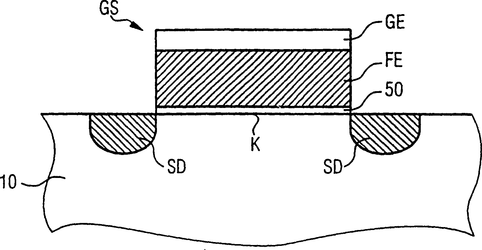
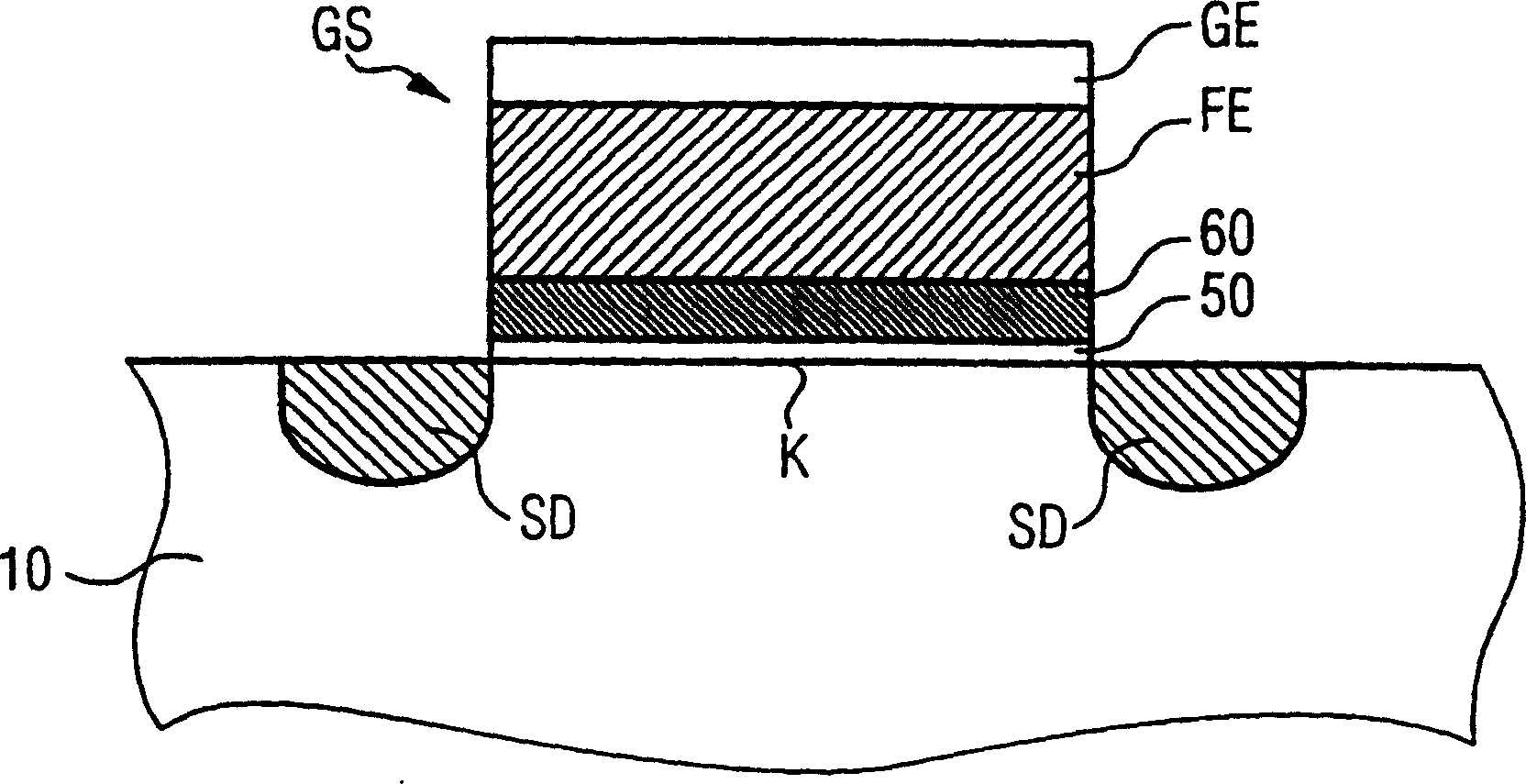
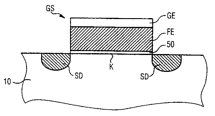
[0027] exist figure 1 Among them, 10 represents the semiconductor substrate, S represents the source region, D represents the drain region, K represents the channel region, GS represents the gate stack, 50 represents the diffusion barrier layer, FD represents the ferroelectric layer and GE means gate.

[0028] High-purity interfaces and silicon nitride (Si 3 N 4 ) combination as a diffusion barrier layer. In modern units, adding hydrofluoric acid vapor to the surface of the substrate can eliminate the natural oxide (SiO2) present on the semiconductor substrate 10. 2 ), followed by Si 3 N 4 The sputtering is carried out without exposing the semiconductor substrate to an oxidizing atmosphere during the two process steps. Therefore, Si can be 3 o 4 Sputtering directly on the semiconductor substrate 10 without having to endure the formation of oxides, especially SiO 2 The reality, depending on the specific circumstances, may also be a ceramic oxide (CeO 2 , Y 2 o 3 , Z...


PUM


Abstract

The present invention relates to a FEMFET device with a semiconductor substrate and to at least one field effect transistor that is provided in the semiconductor substrate. The field effect transistor has a source area, a drain area, a channel area and a gate stack. The gate stack has at least one ferroelectric layer and at least one thin diffusion barrier layer being arranged between the lowest ferroelectric layer and the semiconductor substrate and being configured in such a way that an out-diffusion of the components of the ferroelectric layer into the semiconductor substrate is essentially prevented.

Description

technical field [0001] The invention relates to a ferroelectric memory field effect transistor device (hereinafter referred to as FEMFET) and a manufacturing method thereof. Background technique [0002] The device has: a semiconductor substrate; at least one field effect transistor disposed on the semiconductor substrate and having a source region, a drain region, a channel region and a gate stack (gate stack); The stack has at least one ferroelectric layer; the gate stack (GS) has at least one thin diffusion barrier layer (50), which is arranged on the bottom of the ferroelectric layer (FE) and the semiconductor substrate (10 ) and its configuration structure should basically prevent the components of the ferroelectric layer (or layer) (FE) from diffusing to the semiconductor substrate (10); at least one dielectric buffer layer (60) is arranged on the ferroelectric layer ( FE) and the semiconductor substrate (10) on the gate stack (GS); and the diffusion barrier layer (50...

Claims


Application Information

Patent Timeline
IPC IPC(8): H01L21/8247H01L21/02H01L21/28H01L21/8246H01L27/105H01L29/51H01L29/788H01L29/792
CPCH01L29/516H01L28/56H01L21/28291H01L29/40111H01L27/105
Inventor 蒂尔·施勒塞尔托马斯·彼得·哈内德尔
Owner INFINEON TECH AG
Why Eureka
Try Eureka