Advanced plastic flexible electronic component 3D printing integrated circuit technology
A technology of electronic components and integrated circuits, which is applied in the field of 3D printed integrated circuit technology of flexible electronic components, can solve the problems of too large internal grooves, too thick circuits, and not easy to bend, so as to improve the reaction speed, realize bendability, The effect of reducing the resistance
- Summary
- Abstract
- Description
- Claims
- Application Information
AI Technical Summary
Problems solved by technology
Method used
Image

Examples
Embodiment 1
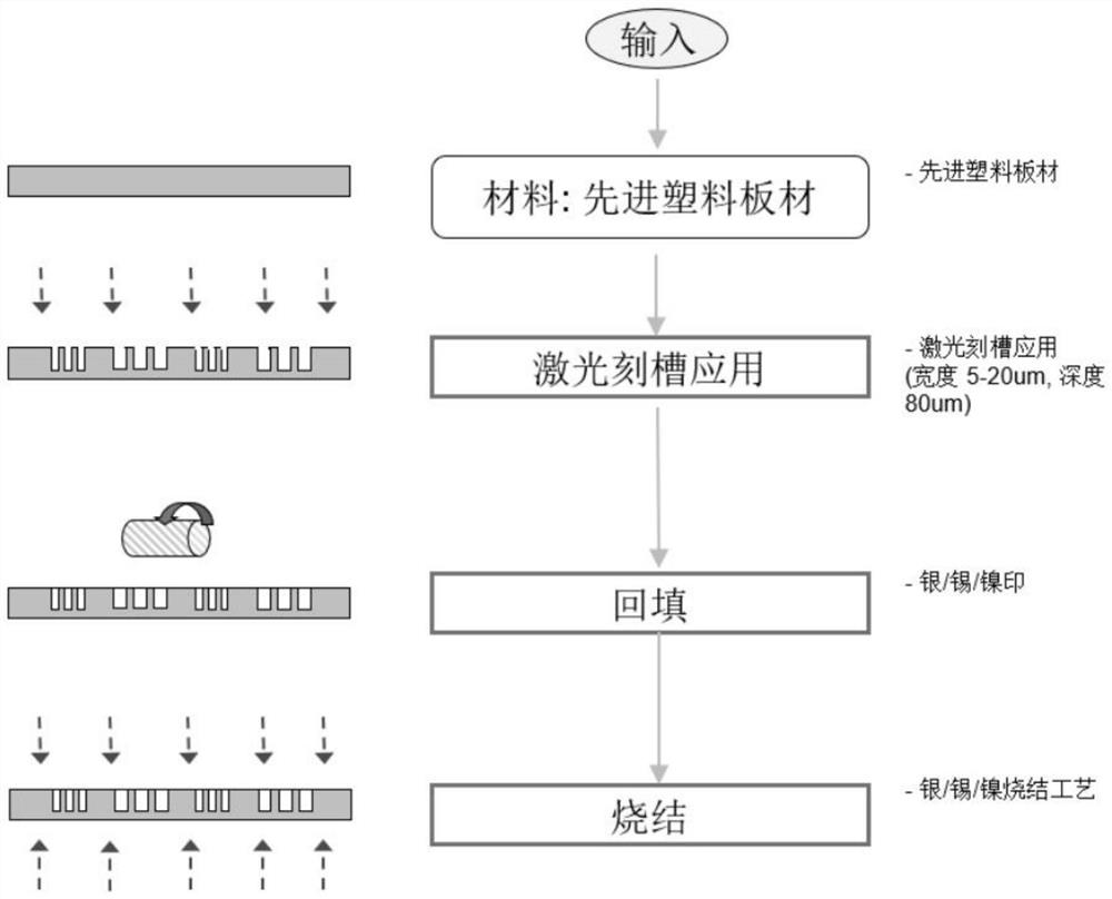
[0045] This embodiment mainly introduces a method for 3D printing integrated circuits of advanced plastic flexible electronic components; please refer to the process flow figure 1 , figure 1 The invention provides a flow chart of an advanced plastic flexible electronic component 3D printing integrated circuit process.
[0046] An advanced plastic flexible electronic component 3D printing integrated circuit process, which includes the following steps:
[0047] Step S1, selecting advanced plastics as the base;
[0048] Step S2, laser mask projection processing the substrate to form deep grooves;
[0049] Step S3, backfilling the metal paste;
[0050] Step S4, sintering the metal paste to form.
[0051] Further, in the step S2, the width of the deep groove is 5-20 microns; the depth of the deep groove is 75-85 microns.
[0052] Further, in the step S2, the inner surface of the deep groove is an uneven plane structure.
[0053] Further, the advanced plastic material includes on
Embodiment 2
[0062] This embodiment mainly introduces an optimal method for the 3D printing integrated circuit process of advanced plastic flexible electronic components.
[0063] An advanced plastic flexible electronic component 3D printing integrated circuit process, which includes the following steps:
[0064] Step S1, selecting advanced plastics as the base;
[0065] Step S2, laser mask projection processing the substrate to form deep grooves;
[0066] Step S3, backfilling the metal paste;
[0067] Step S4, sintering the metal paste to form.
[0068] Further, in the step S2, the width of the deep groove is 12.5 microns; the depth of the deep groove is 80 microns.
[0069] Further, in the step S2, the inner surface of the deep groove is an uneven plane structure.
[0070] Further, the advanced plastic material includes one or two combinations of polyimide or polyethersulfone resin.
[0071] Further, in the step S1, the thickness of the substrate is 100 microns.
[0072] Further, the
Embodiment 3
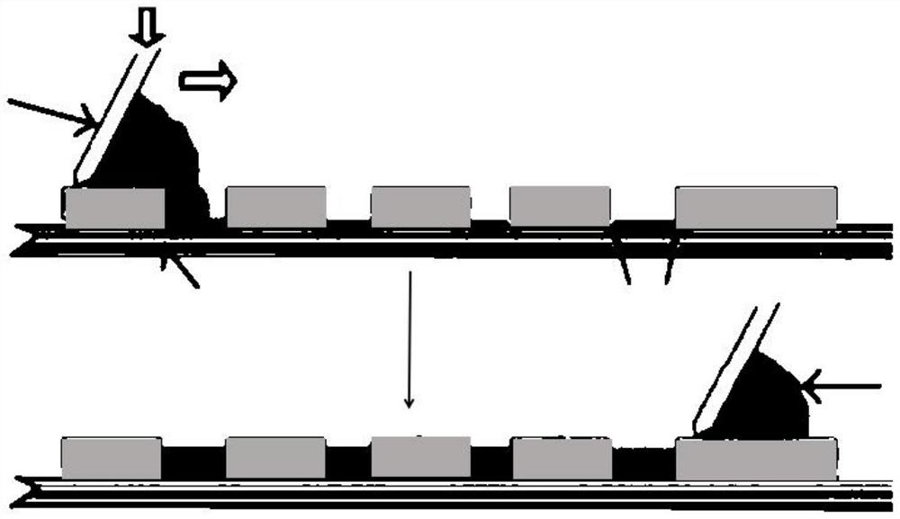
[0075] Based on the above Embodiment 1, this embodiment mainly introduces a method for backfilling metal paste in the 3D printing integrated circuit process of advanced plastic flexible electronic components. For the specific method, please refer to figure 2 , which includes the following steps:
[0076] Step S31, install the front and rear squeegee strips of the 3D printer to ensure that the squeegee is flat, and then install the squeegee bracket;
[0077] Step S32, adjusting the speed and pressure of the 3D printer;
[0078] Step S33 , using a 3D printer to print the metal paste on the pattern substrate for backfilling.
[0079] Further, the front and rear squeegee strips of the 3D printer are squeegee strips with a hardness of 100-150.
[0080] Further, before step S31, the uniform metal paste needs to be rotated.
[0081] Further, the oblique opening of the squeegee is 500 microns;
[0082] Further, the height of metal paste backfill is the same as that of advanced plast
PUM
| Property | Measurement | Unit |
|---|---|---|
| Thickness | aaaaa | aaaaa |
| Depth | aaaaa | aaaaa |
| Depth | aaaaa | aaaaa |
Abstract
Description
Claims
Application Information
 - R&D Engineer
- R&D Manager
- IP Professional
- Industry Leading Data Capabilities
- Powerful AI technology
- Patent DNA Extraction
Browse by: Latest US Patents, China's latest patents, Technical Efficacy Thesaurus, Application Domain, Technology Topic.
© 2024 PatSnap. All rights reserved.Legal|Privacy policy|Modern Slavery Act Transparency Statement|Sitemap