Semiconductor memory device including a capacitor an upper electrode of which being resistant of exfoliation
a memory device and semiconductor technology, applied in semiconductor devices, capacitors, electrical devices, etc., can solve the problems of reducing the manufacturing yield of semiconductor memory devices, reducing the spontaneous polarization, etc., and achieve the effect of quick and easy formation
- Summary
- Abstract
- Description
- Claims
- Application Information
AI Technical Summary
Benefits of technology
Problems solved by technology
Method used
Image

Examples
first embodiment
(First Embodiment)
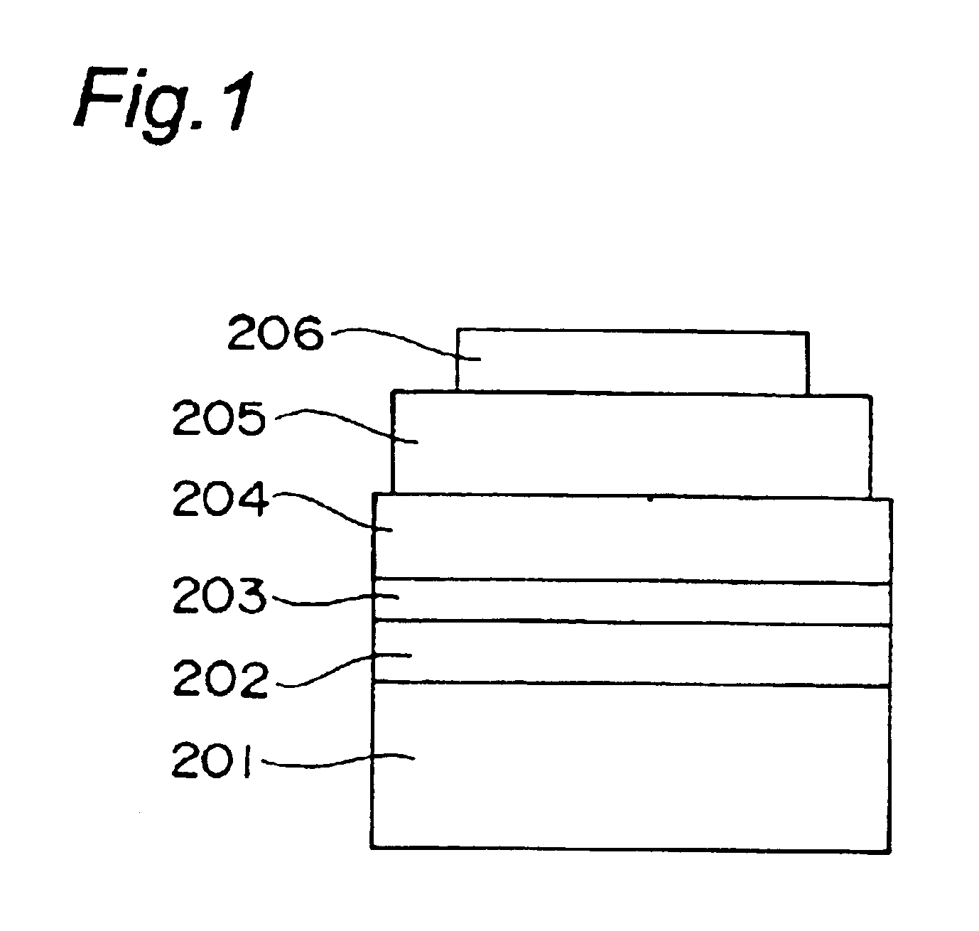
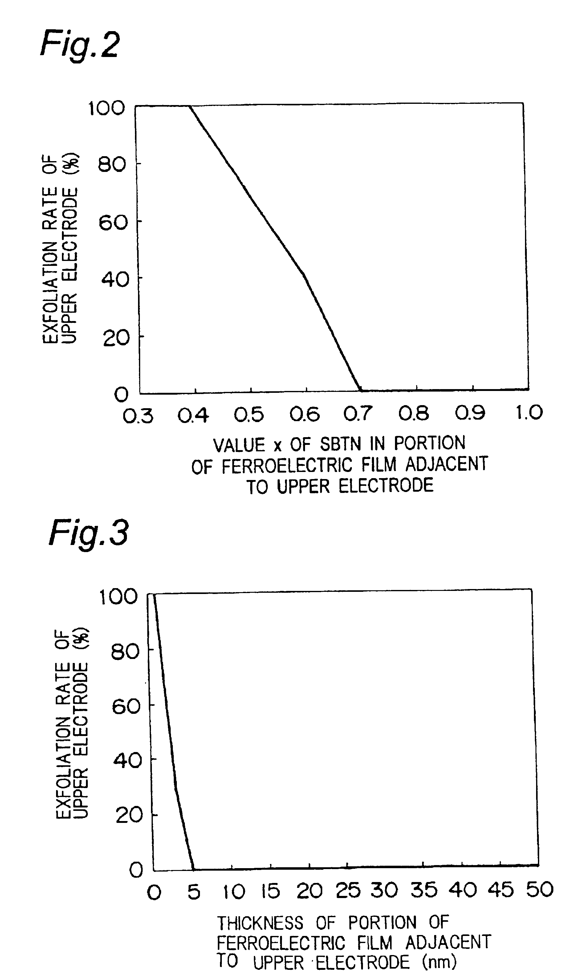
FIG. 1 is a view showing a capacitor provided with a semiconductor memory device of the present invention. The capacitor has a silicon substrate 201, on which a silicon oxide 202, an adhesion layer 203 consisting of TiO2, a lower electrode 204 as a lower electrode film consisting of Pt, a ferroelectric thin film 205 as a dielectric film, and an upper electrode 206 as an upper electrode film consisting of Pt are disposed. In the present embodiment, composition of a portion of the ferroelectric film adjacent to the upper electrode 206 is changed to form eight kinds of different ferroelectric thin films 205, on each of which an upper electrode 206 is formed for performing an experiment about adhesion between the ferroelectric thin film 205 and the upper electrode 206.
First, on a silicon substrate 201, there is formed a silicon oxide 202 with a film thickness of 300 nm by thermal oxidation, on which TiO2 is laminated by sputtering to form an adhesion layer 203. On the adh
second embodiment
(Second Embodiment)
In the second embodiment of the present invention, there are formed ferroelectric films 205 with a portion each having a different value x of SBTN whose thickness is changed for performing an experiments about adhesion of the ferroelectric film 205 and the upper electrode 206. In this embodiment, a capacitor having structure approximately identical to that of FIG. 1 is formed. More particularly, like the first embodiment, on the silicon substrate 201, there are formed a silicon oxide 202, an adhesion layer 203 consisting of TiO2, a lower electrode 204 as a lower electrode film consisting of Pt, a ferroelectric thin film 205 as a dielectric film, and an upper electrode 206 as an upper electrode film consisting of Pt.
In the present embodiment, in forming the ferroelectric thin film 205, first, lamination of an SBN layer with a thickness of 30 nm is repeated 6 times to obtain an SBN film of 180 nm as with the case of forming the ferroelectric film 205 of the first embod
third embodiment
(Third Embodiment)
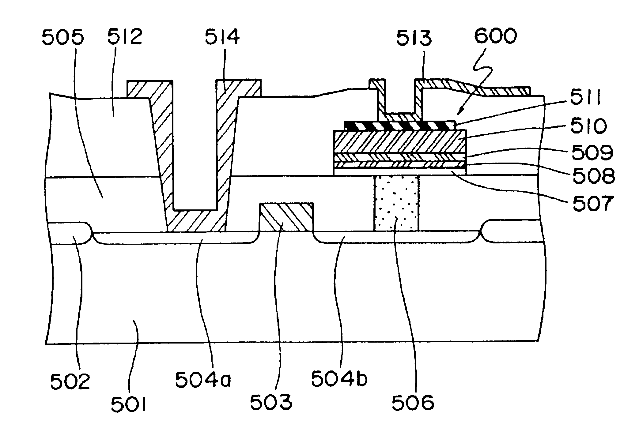
FIG. 4 is a view showing a semiconductor memory device in a third embodiment of the present invention. This semiconductor memory device is a stack-type semiconductor memory device. The semiconductor memory device is formed as shown below. First, on the surface of a silicon substrate 501, there is formed a LOCOS film with a film thickness of approx. 5,000 Å to produce an element isolation area. Next, there is formed a selective transistor composed of a gate electrode 503, a source area 504a, and a drain area 504b, and then a first silicon oxide 505 as an interlayer insulating film is formed to have a thickness of approx. 5,000 Å by a CVD (Chemical Vapor Deposition) method. Then, on the first silicon oxide 505, there is formed a contact hole with a diameter of approx. 0.6 μm, in which polysilicon is embedded by a CVD method. After that, the surface of the polysilicon is planarized by a CMP (Chemical Machine Polishing) method to form a polysilicon plug 506. After the pol
PUM
 Abstract
Description
Claims
Application Information
 - R&D Engineer
- R&D Manager
- IP Professional
- Industry Leading Data Capabilities
- Powerful AI technology
- Patent DNA Extraction
Browse by: Latest US Patents, China's latest patents, Technical Efficacy Thesaurus, Application Domain, Technology Topic.
© 2024 PatSnap. All rights reserved.Legal|Privacy policy|Modern Slavery Act Transparency Statement|Sitemap