Bonding pad layer system, gas sensor and method for manufacturing a gas sensor

a gas sensor and bonding pad technology, applied in the direction of instruments, fluid speed measurement, coatings, etc., can solve the problem of system lack of process stability, achieve the effects of reducing material consumption, reducing material consumption, and preventing the diffusion behavior of atoms

Active Publication Date: 2020-05-07
ROBERT BOSCH GMBH
View PDF0 Cites 0 Cited by
  • Summary
  • Abstract
  • Description
  • Claims
  • Application Information

AI Technical Summary

Benefits of technology

The present invention relates to improving the performance of tantalum nitride films used in electronic devices such as capacitors. By controlling the diffusion properties of atoms within the tantalum nitride film, the device can have improved efficiency and reduced energy usage compared to traditional methods like vacuum evaporation. Additionally, the use of specific compositions of the tantalum and first platinum layers helps improve their durability and reliability. Overall, these improvements lead to better performance and cost savings in electronic devices.

Problems solved by technology

The technical problem addressed by this patent is how to improve the performance and reliability of gas sensors while maintaining their functionality over time without losing any function or causing damage from environmental factors.

Method used


Image

  • Bonding pad layer system, gas sensor and method for manufacturing a gas sensor
  • Bonding pad layer system, gas sensor and method for manufacturing a gas sensor
  • Bonding pad layer system, gas sensor and method for manufacturing a gas sensor

Examples


Embodiment Construction

[0029]Identical reference numerals in the figures refer to identical or functionally identical elements.

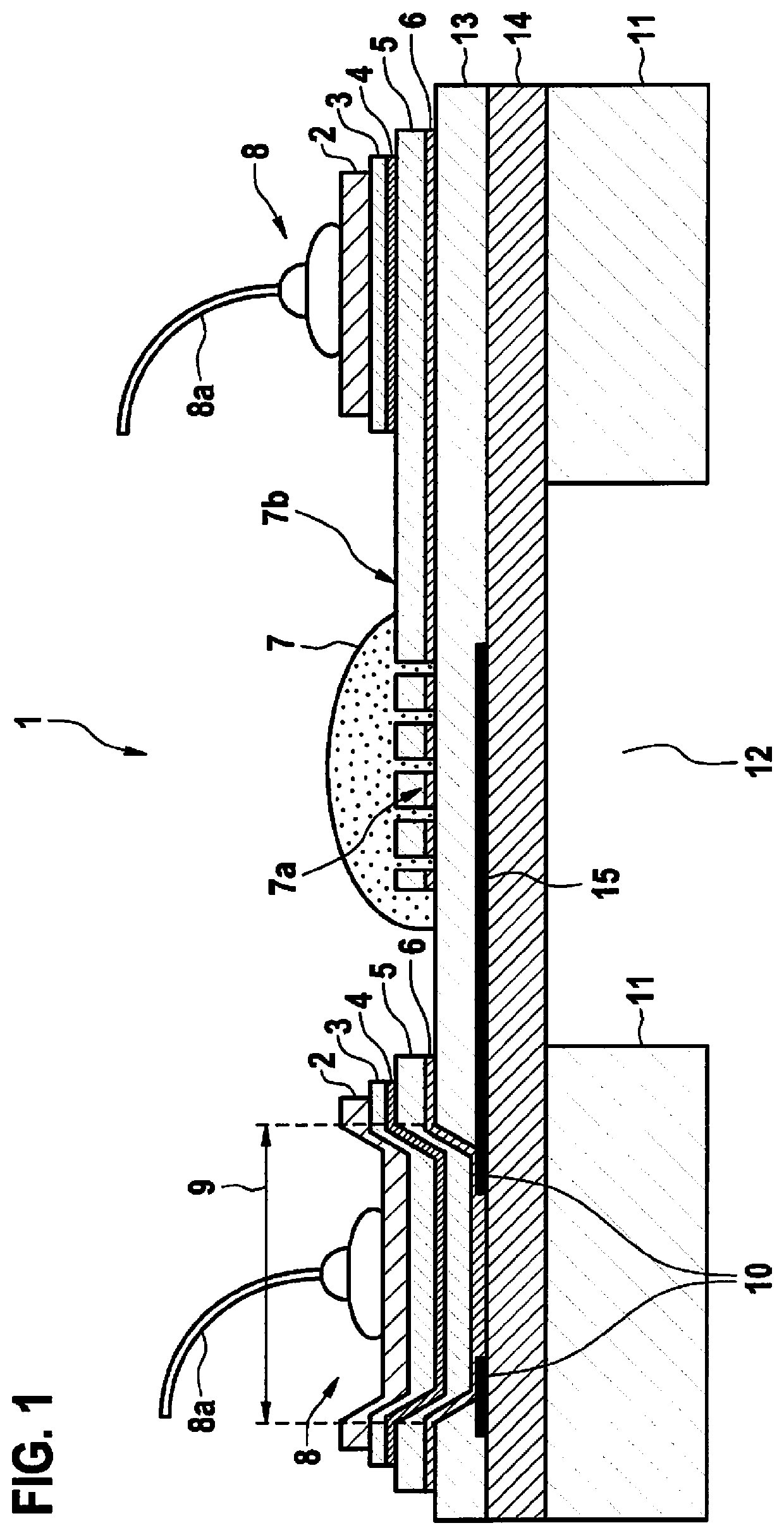
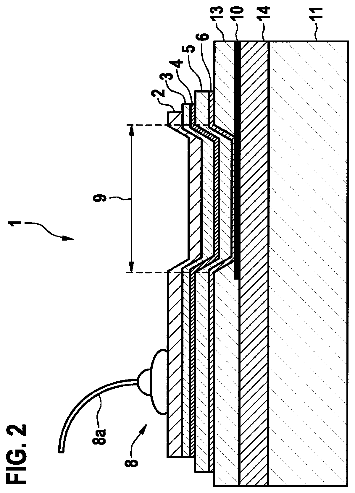
[0030]FIG. 1 is a schematic representation of a gas sensor according to a first specific embodiment of the present invention.

[0031]One possible implementation of a gas sensor according to the present invention is shown, including a bonding path layer system 1, including a micromechanical semiconductor chip 11 having a cavern 12 as a base, two dielectric layers 13 and 14, a platinum conductor track 10 to heater 15 in cavern area 12, a tantalum layer 6, upon which a first platinum layer 5 is deposited, upon that a tantalum nitride layer 4 is deposited, upon that a second platinum layer 3 is deposited, upon that a gold layer 2 is deposited, the individual layers being deposited over the entire area, even over a contact hole 9 and the individual layers subsequently being structured with the aid of standard methods. A bonding pad 8, a bonding wire 8a, a paste dot 7 and schematically an el


PUM

PropertyMeasurementUnit
Temperatureaaaaaaaaaa
Thicknessaaaaaaaaaa
Thicknessaaaaaaaaaa

Abstract

A bonding pad layer system is deposited on a semiconductor chip as a base, for example, a micromechanical semiconductor chip, in which at least one self-supporting dielectric membrane made up of dielectric layers, a platinum conductor track and a heater made of platinum is integrated. In the process, the deposition of a tantalum layer takes place first, upon that the deposition of a first platinum layer, upon that the deposition of a tantalum nitride layer, upon that the deposition of a second platinum layer and upon that the deposition of a gold layer, at least one bonding pad for connecting with a bonding wire being formed in the gold layer. The bonding pad is situated in the area of the contact hole on the semiconductor chip, in which a platinum conductor track leading to the heater is connected using a ring contact and/or is connected outside this area.

Description


Claims


Application Information

Patent Timeline
Owner ROBERT BOSCH GMBH
Why Eureka
Try Eureka