Method of manufacturing printed circuit board, and printed circuit board obtained using method of manufacturing printed circuit board
A technology for printed circuit boards and manufacturing methods, which is applied in the fields of printed circuit manufacturing, printed circuits, and secondary treatment of printed circuits, etc., can solve problems such as difficulty in ensuring long-term reliability of printed circuit boards, surface layer movement, etc., and achieve excellent movement resistance, Excellent effect in terms of flat surface and stability in use
- Summary
- Abstract
- Description
- Claims
- Application Information
AI Technical Summary
Problems solved by technology
Method used
Image

Examples
Embodiment 1
[0067] Manufacture of Copper Clad Laminates
[0068] On both sides of a material obtained by laminating three layers of prepreg (GHPL830-NS: manufactured by Mitsubishi Gas Chemical Co., Ltd.) with a thickness of 0.1mm, the non-rough surface roughness (ten-point average roughness Rzjis) of the overlapping pair is 0.37μm. Non-roughened copper foil with a primer resin layer (MFG-DMT3F: manufactured by Mitsui Metal Mining Co., Ltd.) made by coating copper foil with a primer resin, and then processed by a vacuum press at a temperature of 220°C and a pressure of 4.0MP. 90 minutes of forming to produce a copper clad laminate with a thickness of 0.3 mm.
[0069] Manufacturing of printed circuit boards
[0070] Printed circuit boards are manufactured using a semi-additive method. About the manufacturing process of this printed wiring board, an Example and a comparative example are common. Form an electroplating resist layer on the surface of the outer layer copper foil of the above-...
Embodiment 2
[0078] In Example 2, the non-roughened copper foil with a primer resin layer used in Example 1 was changed from MFG-DMT3F manufactured by Mitsui Metal Mining Co., Ltd. to PF-E-3 manufactured by Hitachi Chemical Industries, Ltd., except Otherwise, printed wiring board samples were produced in the same manner as in Example 1.
[0079]The above-mentioned printed wiring board sample was subjected to cleaning treatment in the same manner as in Example 1 to prepare a cleaning treatment sample, and semi-quantitative analysis was performed on the amount of residual metal components on the surface of the insulating resin layer exposed between circuits in the cleaning treatment sample. , and then determine the surface roughness (Rzjis). In addition, in the same manner as in Example 1, the occurrence of delamination was evaluated. The surface state of the insulating resin layer exposed between the circuits is shown in Table 1 below, and the evaluation results of delamination and cleanin...
Embodiment 3
[0081] In Example 3, using the sample of the printed wiring board produced in Example 1, only the cleaning treatment conditions were changed.
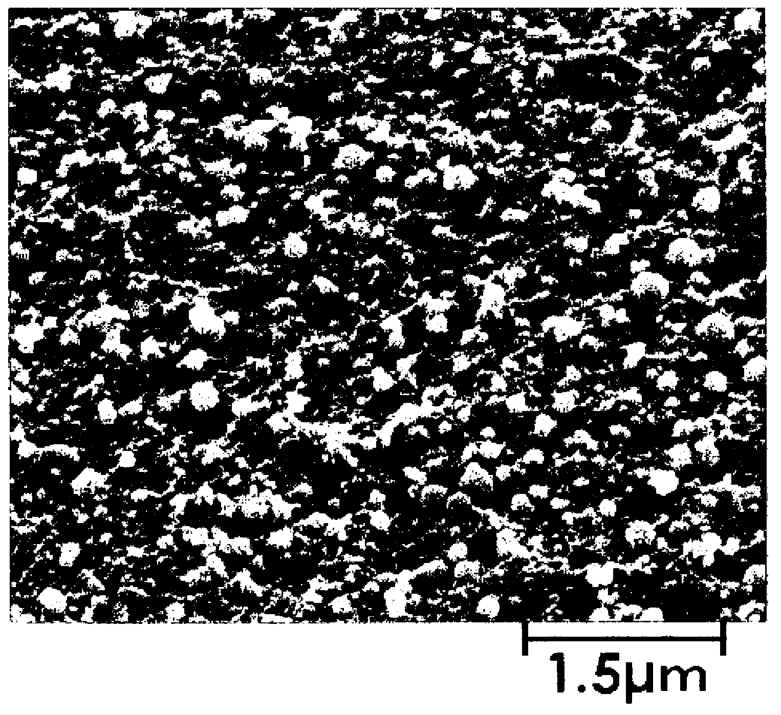
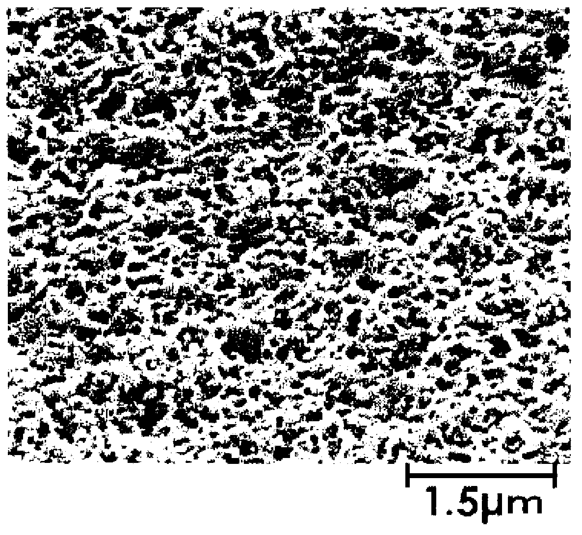
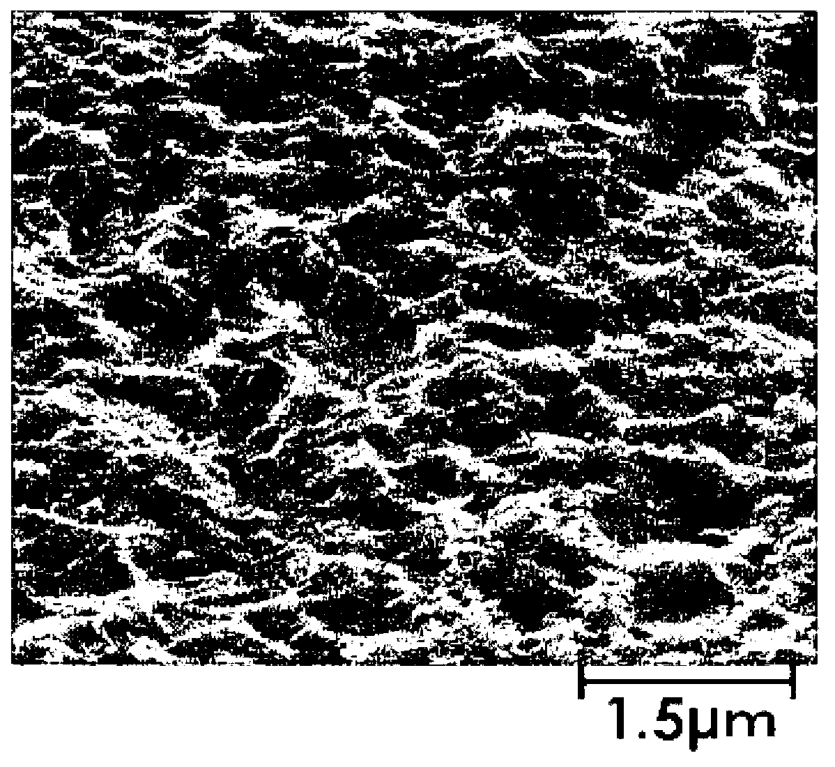
[0082] In the purification process, the sample of the above-mentioned printed circuit board was plasma etched under the condition of input energy of 40J / cm2 in a chamber of [(CF4 partial pressure) / (O2 partial pressure)]=0.33 and air pressure of 15Pa. Next, immerse for 5 minutes in a 10% by mass solution of sulfuric acid as an acid component and Melplate PC-316 (manufactured by Melplate Co., Ltd.) containing ethylene glycol as a surfactant, and after washing, spray a microetching solution (CZ8101B: manufactured by MEG Co., Ltd.) for 30 seconds, washed with water, and dried to prepare a purified sample. image 3 Shown is a scanning electron microscope observation image of the surface of the insulating resin layer exposed between the circuits immediately after the circuit is formed, figure 2 Shown is a scanning electron microscope obser...
PUM
 Abstract
Description
Claims
Application Information
 - R&D Engineer
- R&D Manager
- IP Professional
- Industry Leading Data Capabilities
- Powerful AI technology
- Patent DNA Extraction
Browse by: Latest US Patents, China's latest patents, Technical Efficacy Thesaurus, Application Domain, Technology Topic.
© 2024 PatSnap. All rights reserved.Legal|Privacy policy|Modern Slavery Act Transparency Statement|Sitemap