Methods of producing seed crystal substrates and group 13 element nitride crystals, and seed crystal substrates

Active Publication Date: 2017-12-28
NGK INSULATORS LTD
View PDF4 Cites 0 Cited by
  • Summary
  • Abstract
  • Description
  • Claims
  • Application Information

AI Technical Summary

Benefits of technology

The patent text describes a method to improve the quality and yield of growing nitride crystals on a substrate. The invention introduces a method that reduces cracks in the nitride crystal and improves the production yield by growing a crystal of a nitride of a group 13 element on a seed crystal substrate, where an altered portion is formed to prevent cracks. The crystal can be easily separated from the supporting body with reduced cracks, leading to improved yield. Additionally, the bowing of the substrate is improved, which facilitates the growth of nitride crystals with better quality.

Problems solved by technology

However, according to the production methods of patent documents 1 and 2, it is left parts where the gallium nitride layer and supporting body are not spontaneously separated and are adhered to each other, resulting in reduction of a production yield.
Particularly, as the area of the supporting body becomes large, the increase of the cracks or bowing tends to be observed, which is problematic.
However, this method provides a template substrate having the supporting body and the gallium nitride layer integrated with it, and does not provide a free-standing substrate composed of the gallium nitride layer.
For preventing the disappearance of the seed crystal layer, it is necessary to form the seed crystal film again by vapor phase growing method, which is problematic.

Method used


Image

  • Methods of producing seed crystal substrates and group 13 element nitride crystals, and seed crystal substrates
  • Methods of producing seed crystal substrates and group 13 element nitride crystals, and seed crystal substrates
  • Methods of producing seed crystal substrates and group 13 element nitride crystals, and seed crystal substrates

Examples


examples a1

to A7

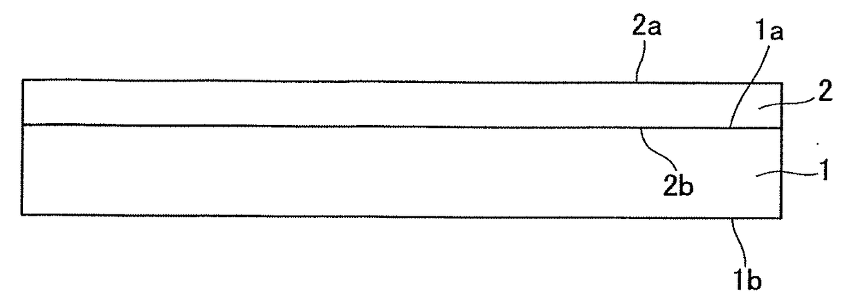
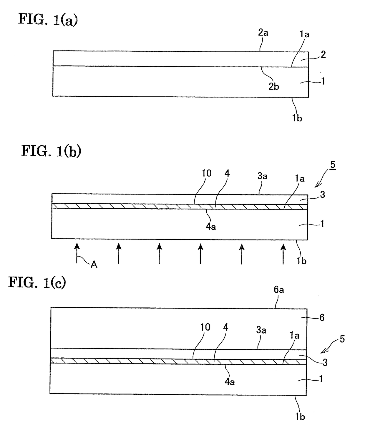
[0075]A c-plane body 1 of sapphire single crystal with a diameter of 4 or 6 inches and a thickness of 1.3 mm was put in an MOCVD apparatus (metal organic chemical vapor deposition apparatus), and heated at 1150° C. for 10 minutes in hydrogen atmosphere to perform the cleaning of the surface of the body. Then, the temperature of the body was lowered to 500° C., and the gallium nitride layer was grown to a thickness of 20 nm using TMG (trimethyl gallium) and ammonia as raw materials to provide the underlying layer. Next, the temperature of the body was raised up to 1100° C., and a seed crystal layer 2 of gallium nitride was grown to a thickness of 4 μm using TMG and ammonia as raw materials.

[0076]Then, laser light was irradiated from the side of the sapphire body 1 to form the altered portion.

[0077]As a laser light source, it was used a pulse laser using a third harmonic wave (wavelength of 355 nm) of Nd:YAG laser. The repetition frequency was made 10 Hz, the pulse width was made...

example b1

[0091]The seed crystal substrate was produced and gallium nitride layer was grown thereon as the Example A3. Then, the supporting body was processed by grinding so that the gallium nitride crystal layer was separated to obtain a free-standing substrate. Then, the yield of the cooling step, the yield of the separation by grinding and amount of bowing of the free-standing substrate after the separation were measured and shown in table 2.

examples c1 to c6

[0094]The seed crystal substrate was produced and gallium nitride crystal layer was grown as the Example A. However, according to the present examples, the thickness of the gallium nitride layer was made as large as 1400 μm, so that the gallium nitride crystal layer was separated from the supporting body due to spontaneous separation during the cooling step.


PUM


Abstract

A seed crystal layer is provided on a supporting body. A laser light is irradiated from a side of the supporting body to provide an altered portion along an interface between the supporting body and seed crystal layer. The altered layer is composed of a nitride of a group 13 element and comprising a portion into which dislocation defects are introduced or an amorphous portion.

Description

CROSS-REFERENCE TO RELATED APPLICATIONS[0001]This is a continuation of International Application No. PCT / JP2017 / 000948, filed Jan. 13, 2017, which claims priority of Japanese Patent Application No. 2016-060185, filed Mar. 24, 2016, the entire contents of which are incorporated herein by reference.TECHNICAL FIELD[0002]The present invention relates to a seed crystal substrate for growing gallium nitride or the like, a method of producing the same and a method of producing a crystal of a nitride of a group 13 element.BACKGROUND ARTS[0003]According to patent document 1, it is proposed to form an intermediate layer with a low hardness on a sapphire substrate, to form a seed crystal substrate of gallium nitride thereon and to grow a thick film of gallium nitride by flux method. The thick film of gallium nitride is separated from the sapphire substrate during the cooling step.[0004]Further, according to patent document 2, when a seed crystal film is formed on a sapphire substrate, voids ar...

Claims


Application Information

Patent Timeline
IPC IPC(8): H01L21/02C30B1/02C30B29/40C30B33/08
CPCH01L21/0254C30B1/023C30B33/08C30B29/406C30B19/02C30B19/12C30B33/06H01L21/0242H01L21/02458H01L21/0262H01L21/02694
Inventor SAKAI, MASAHIROYOSHINO, TAKASHI
Owner NGK INSULATORS LTD
Why Eureka
Try Eureka