Thin circuit board structure

A technology of circuit board and build-up structure, applied in the direction of circuit substrate materials, circuits, printed circuits, etc., can solve the problems of signal noise, electrical characteristics limitation, unfavorable signal transmission, etc., to reduce parasitic capacitance and inductance, and improve electrical characteristics. , the effect of reducing manufacturing costs

Inactive Publication Date: 2007-05-30
PHOENIX PRECISION TECH CORP
View PDF0 Cites 3 Cited by
  • Summary
  • Abstract
  • Description
  • Claims
  • Application Information

AI Technical Summary

Problems solved by technology

The parasitic impedance will have a negative impact on the transmission of the signal, resulting in the lack of integrity of the signal transmission (Integrity), that is, the signal contains noise (noise), which affects the correctness of the signal transmission
High-speed and high-frequency circuits are more affected by noise, which is not conducive to signal transmission and limits the improvement of electrical characteristics
[0007] In addition, the circuit board used for semiconductor packaging is a symmetrical circuit build-up layer structure 13 on the two surfaces of the core board 11. The symmetrical structure is not absolutely necessary, so increasing the number of redundant layers will increase the production cost on the one hand, and on the other hand. The purpose of thinning the circuit cannot be achieved due to the increase in the number of layers

Method used


Image

  • Thin circuit board structure
  • Thin circuit board structure

Examples


Embodiment

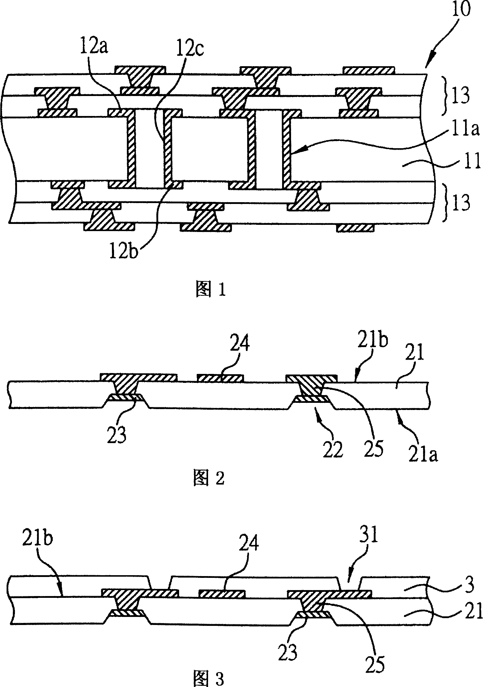
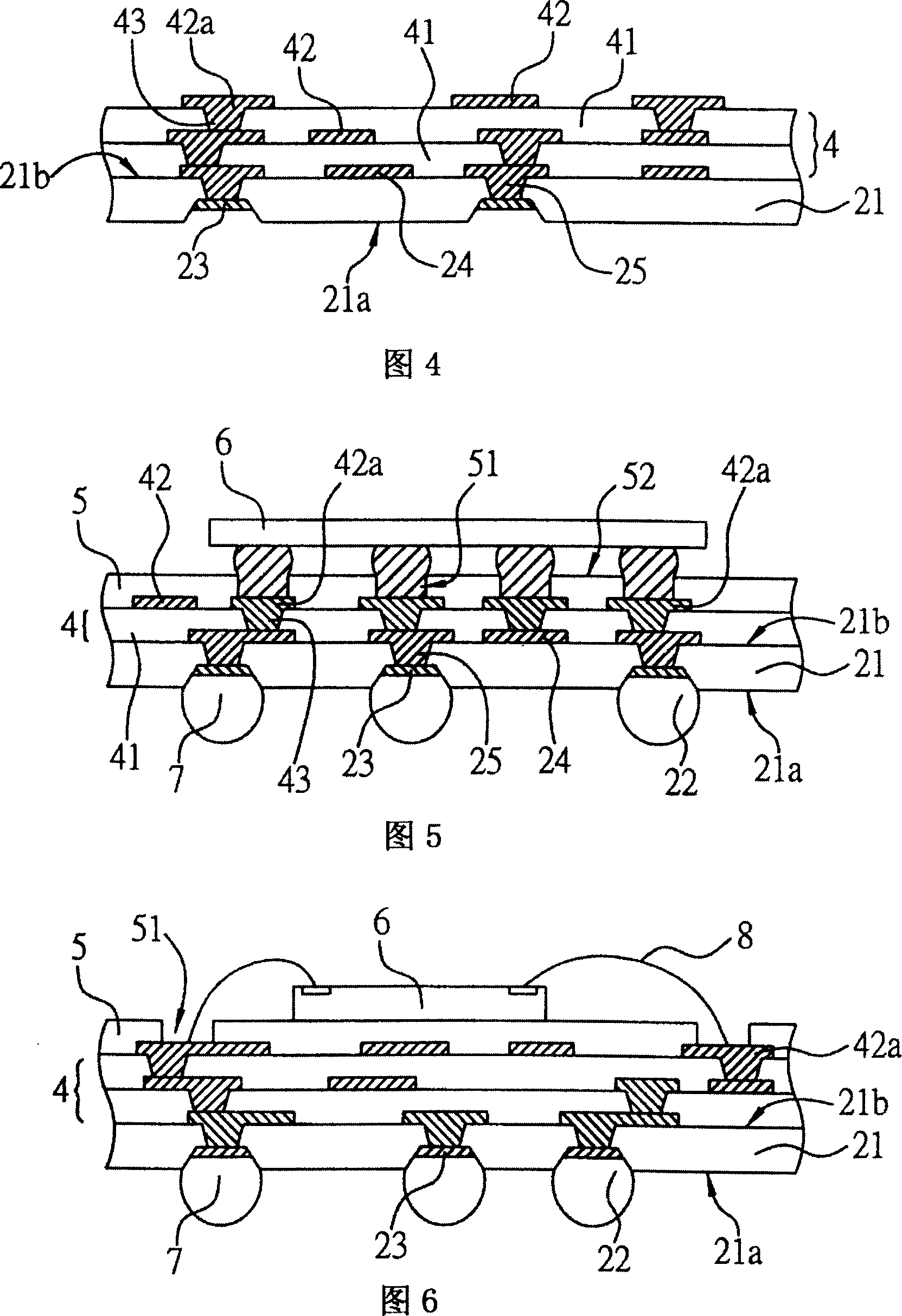
[0025] Please refer to FIG. 2 , which is a schematic cross-sectional view of a thinned circuit board structure according to the present invention. The thinned circuit board structure includes: a dielectric layer 21 forming at least one recessed area 22 on a surface 21a thereof. The dielectric layer 21 It is a dielectric material, and the dielectric layer 21 is, for example, a soft board or a hard board made of organic polymer materials, ceramic materials, polymer materials filled with ceramic powder, etc.; a metal pad 23 is formed in the recessed area In 22, the metal pad 23 is selected from gold, nickel, palladium, silver, tin, nickel / palladium, chromium / titanium, nickel / gold, copper / nickel / gold, palladium / gold, nickel / palladium / gold, copper, tin, Nickel, chromium, titanium, copper / chromium alloy or tin / lead alloy; at least one circuit layer 24, formed on the other surface 21b of the dielectric layer 21; and a plurality of conductive blind holes 25, formed in the dielectric la...


PUM


Abstract

This invention relates to one thin circuit board structure, which comprises the following parts: one medium layer with at least one concave area; one metal pad into concave area; at least one circuit layer on other surface of medium layer; multiple conductive blind holes in medium layer to supply connection between circuit layer and metal pad. This invention does not use core board and electricity coating hole to contract circuit resistance with high intensity sealing.

Description

technical field [0001] The invention relates to a thinned circuit board structure, in particular to a thinned circuit board without using a core board. Background technique [0002] With the vigorous development of the electronics industry, electronic products are gradually developing in the direction of multi-function and high performance. In order to meet the packaging requirements of high integration and miniaturization of semiconductor packages, the performance of a single semiconductor package is improved. , in line with the trend and demand for miniaturization, large capacity and high speed of electronic products, most of them adopt multi-chip modular (Multi Chip Module; MCM) package form, which can also reduce the volume of the overall package and improve Electrical functions have become the mainstream of packaging. The circuit board that provides active and passive components and line connection has also evolved from a double-layer circuit board to a multi-layer cir...

Claims


Application Information

Patent Timeline
IPC IPC(8): H05K1/00H05K1/03H05K1/09H05K1/11H05K1/02H01L23/48
CPCH01L2224/16225H01L2224/48091H01L2224/48228H01L2924/15311
Inventor 许诗滨
Owner PHOENIX PRECISION TECH CORP
Why Eureka
Try Eureka